- October 14, 2025
- PCB Assembly, PCB Blog
Common PCB Assembly Defects and How to Prevent Them
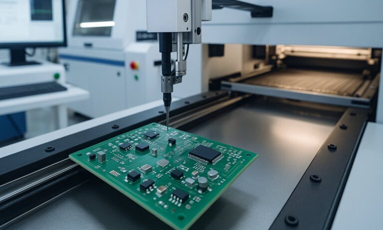
At Precision4PCB, quality and precision are at the core of every circuit we produce. PCB assembly is a highly intricate process that demands accuracy, consistency, and control. Even the smallest soldering error can result in major performance failures or costly rework.
To maintain top-tier reliability, it’s essential to understand the most common PCB assembly defects, their root causes, and the best practices to prevent them.
In this article, we’ll explore three of the most frequent and impactful assembly defects: solder bridging, tombstoning, and cold solder joints – along with proven methods to eliminate them from your manufacturing process.
Table of Contents
- Understanding PCB Assembly Defects
- Solder Bridging
- Tombstoning
- Cold Solder Joints
- Best Practices for Preventing PCB Defects
- Precision4PCB’s Approach to Quality Assurance
- Conclusion
Understanding PCB Assembly Defects
PCB assembly defects occur when solder joints, components, or conductive paths fail to meet quality and electrical performance standards. These defects often arise during solder paste printing, component placement, or reflow soldering processes.
While advanced machinery minimizes manual error, subtle variations in process parameters or materials can still lead to defects.
Key categories of PCB assembly defects include:
- Solder bridging
- Tombstoning
- Cold solder joints
- Insufficient solder
- Component misalignment
- Voiding
For the purpose of this article, we’ll focus on three that directly impact electrical reliability – solder bridging, tombstoning, and cold solder joints.
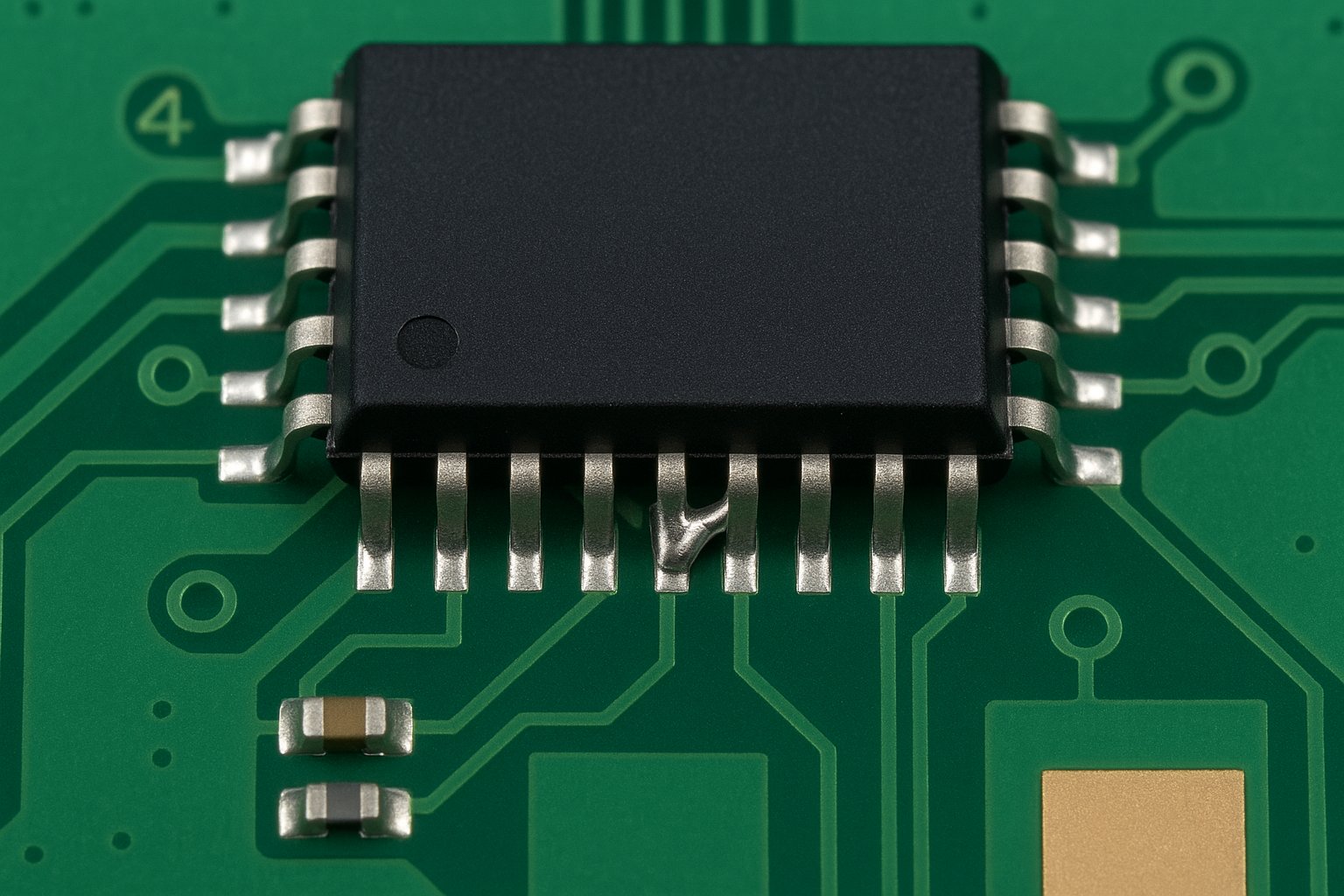
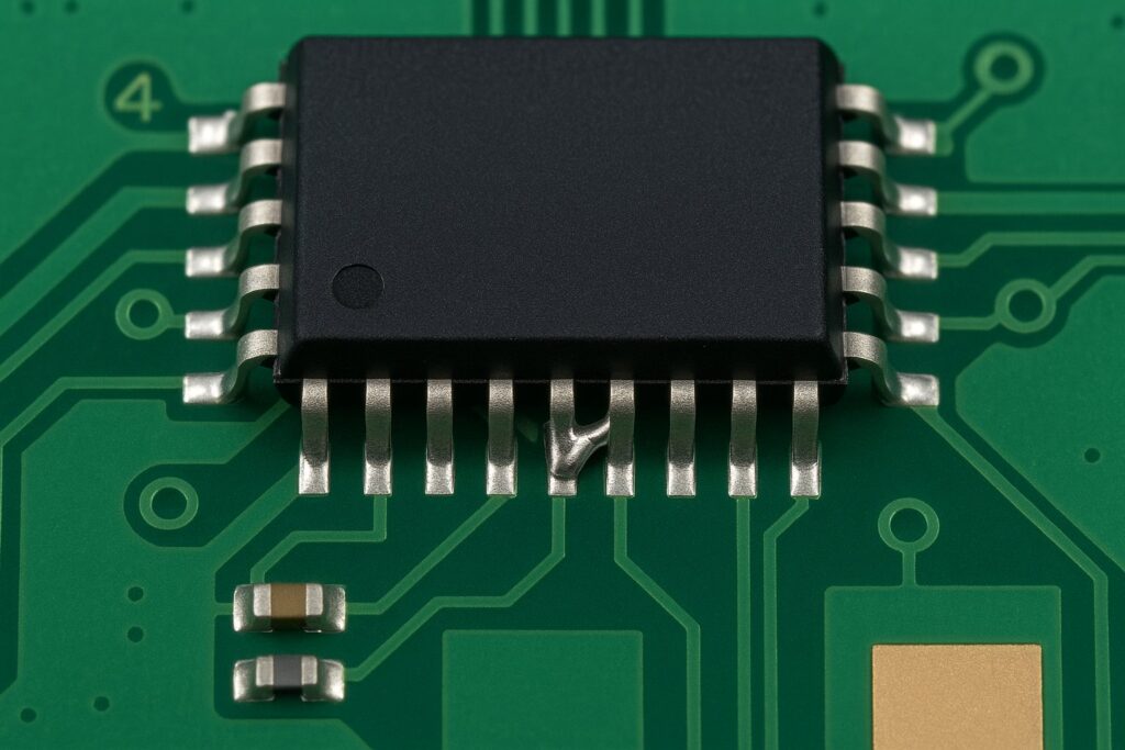
1. Solder Bridging (What Is Solder Bridging?)
Solder bridging occurs when excess solder connects two or more adjacent pads or component leads, creating an unintended electrical short circuit.
Common Causes
- Excessive solder paste application during stencil printing
- Poor stencil design (incorrect aperture size or spacing)
- Insufficient solder mask separation between pads
- Component shifting during reflow
- Improper reflow temperature profile, causing solder to flow excessively
Visual Indicators
- Tiny metallic bridges between leads or pads
- Short circuits detected during electrical testing
- Inconsistent solder fillets under microscope inspection
How to Prevent Solder Bridging
- Use a proper stencil thickness (typically 100–150 µm) to control solder volume
- Optimize stencil aperture design to match pad dimensions
- Maintain clean and precise solder mask dams between pads
- Calibrate pick-and-place accuracy to avoid misalignment
- Fine-tune the reflow oven temperature profile for controlled solder flow
- Conduct AOI (Automated Optical Inspection) immediately after reflow
2. Tombstoning (What Is Tombstoning?)
Tombstoning, also known as the “Manhattan effect,” occurs when one end of a small surface-mount component (usually a resistor or capacitor) lifts from the pad during reflow, leaving it standing vertically – like a tombstone.
Common Causes
- Unequal heating between the two pads during reflow
- Uneven solder paste volume across component pads
- Asymmetric pad design (different copper areas or mask clearances)
- Incorrect component placement pressure
- Rapid heating or poor thermal balance in reflow profile
Visual Indicators
- One side of the SMD component lifted or missing contact with the pad
- Open circuit on one end
How to Prevent Tombstoning
- Design symmetrical pads with equal solder mask clearance
- Ensure consistent solder paste deposition on both pads
- Use reflow profiles with controlled heating rates
- Verify component alignment and placement pressure
- Select solder paste with balanced wetting performance
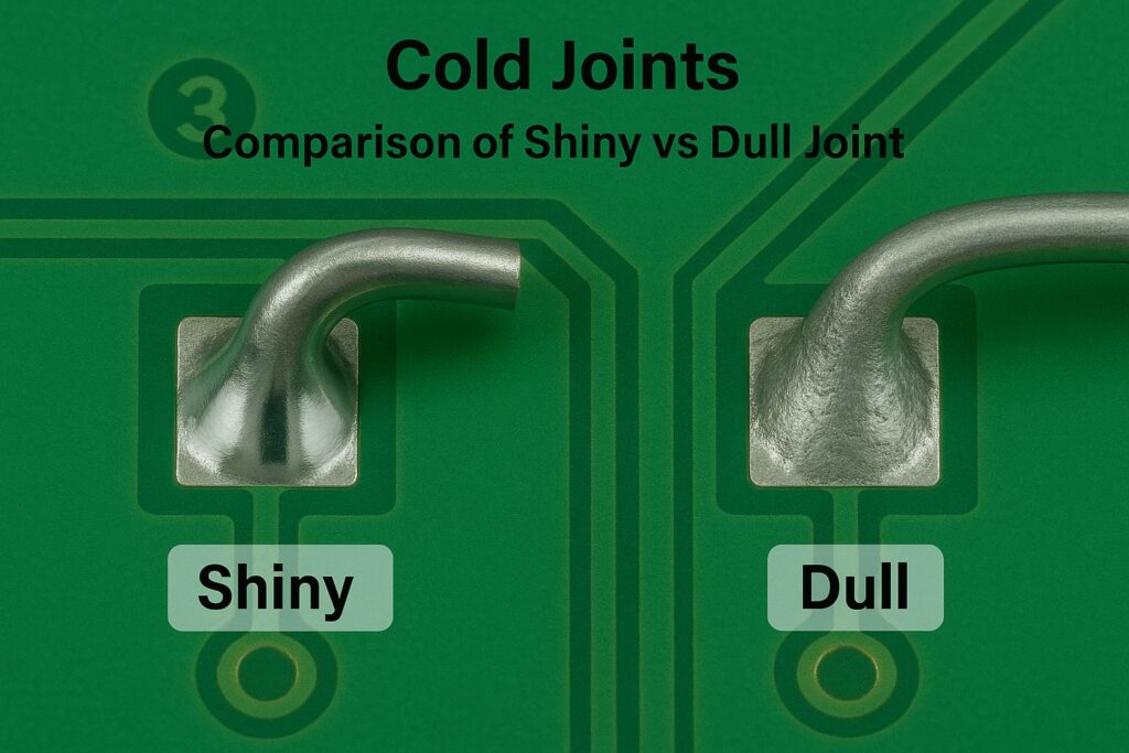
3. Cold Solder Joints (What Are Cold Solder Joints?)
A cold solder joint occurs when solder fails to melt completely or doesn’t properly wet the surfaces, resulting in weak mechanical and electrical bonding.
Solder bridging occurs when excess solder connects two or more adjacent pads or component leads, creating an unintended electrical short circuit.
Common Causes
- Insufficient heat during soldering or reflow
- Contaminated surfaces (oxidation, oil, or flux residue)
- Poor solder paste or flux quality
- Improper manual soldering technique
- Thermal imbalance in reflow process
Visual Indicators
- Dull or grainy surface texture
- Cracked or porous solder joints
- Intermittent connectivity under testing
How to Prevent Cold Solder Joints
- Maintain consistent reflow temperature profiles
- Clean component leads and PCB pads before soldering
- Use high-quality solder paste and flux
- Train operators for proper manual rework techniques
- Inspect using X-ray or AOI to detect hidden defects
Best Practices for Preventing PCB Defects
Preventing assembly defects starts long before production begins. Implementing these best practices can dramatically improve yield and reliability:
1. Design for Manufacturability (DFM)
- Maintain optimal pad geometries and spacing
- Avoid over-dense component layouts
- Use thermal reliefs for balanced soldering
2. Maintain Process Control
- Regularly calibrate stencil printers, pick-and-place, and reflow ovens
- Control environmental conditions – humidity, temperature, and cleanliness
3. Implement Advanced Inspection
- Use AOI to identify bridging, misalignment, or missing parts
- Use X-ray inspection for hidden solder joint verification (especially BGAs)
4. Operator Training
- Continuous technician training ensures correct manual soldering, rework, and inspection standards
Precision4PCB’s Approach to Quality Assurance
At Precision4PCB, our quality control processes are built to eliminate assembly defects before they occur.
Our in-house procedures include:
- 100% optical inspection after solder paste printing and reflow
- Automated X-ray inspection for complex assemblies
- Temperature-profile validation for every reflow batch
- Design review and DFM analysis before production
- Traceability systems for components and solder lots

By combining experienced engineers, advanced equipment, and rigorous inspection, we ensure that every PCB assembly leaving our facility meets the highest industry standards.
Conclusion
Common PCB assembly defects like solder bridging, tombstoning, and cold solder joints can compromise product performance and reliability. Through careful design, controlled processes, and consistent inspection, these issues can be effectively eliminated.
At Precision4PCB, our commitment to excellence ensures that every board we assemble delivers precision, performance, and durability – because in electronics, every connection counts.
Ready to Eliminate PCB Assembly Defects for Good?
At Precision4PCB, we combine advanced manufacturing technology, rigorous inspection systems, and expert engineering to deliver defect-free PCB assemblies – every time.
Whether you need prototype builds, mass production, or design optimization, our team ensures the highest quality and performance at every step.
Contact Precision4PCB today to discuss your PCB assembly requirements or request a free design-for-manufacturability (DFM) review.
Frequently Asked Questions (FAQs)
The most common defects include solder bridging, tombstoning, cold solder joints, insufficient solder, and component misalignment. These issues typically occur during the soldering or reflow process and can impact the electrical reliability of the final product.
Solder bridging happens when excess solder connects adjacent pads or leads, forming an unintended short circuit. Common causes include too much solder paste, poor stencil design, or misalignment during reflow soldering.
Tombstoning can be prevented by maintaining symmetrical pad design, ensuring equal solder paste volume, and using a controlled reflow temperature profile to achieve uniform heating. Proper component placement and high-quality solder paste also help.
Cold solder joints occur when solder fails to properly melt or bond, resulting in weak or intermittent electrical connections. They often appear dull or cracked and can cause signal instability or long-term failure. Maintaining the correct temperature and using clean surfaces prevents this defect.
Precision4PCB uses automated optical inspection (AOI), X-ray verification, and process control validation at every assembly stage. We also conduct DFM reviews, maintain temperature calibration, and ensure operator training to minimize human error and guarantee quality output.