- March 25, 2026
- PCB Blog
The Ins and Out of Controlled Impedance
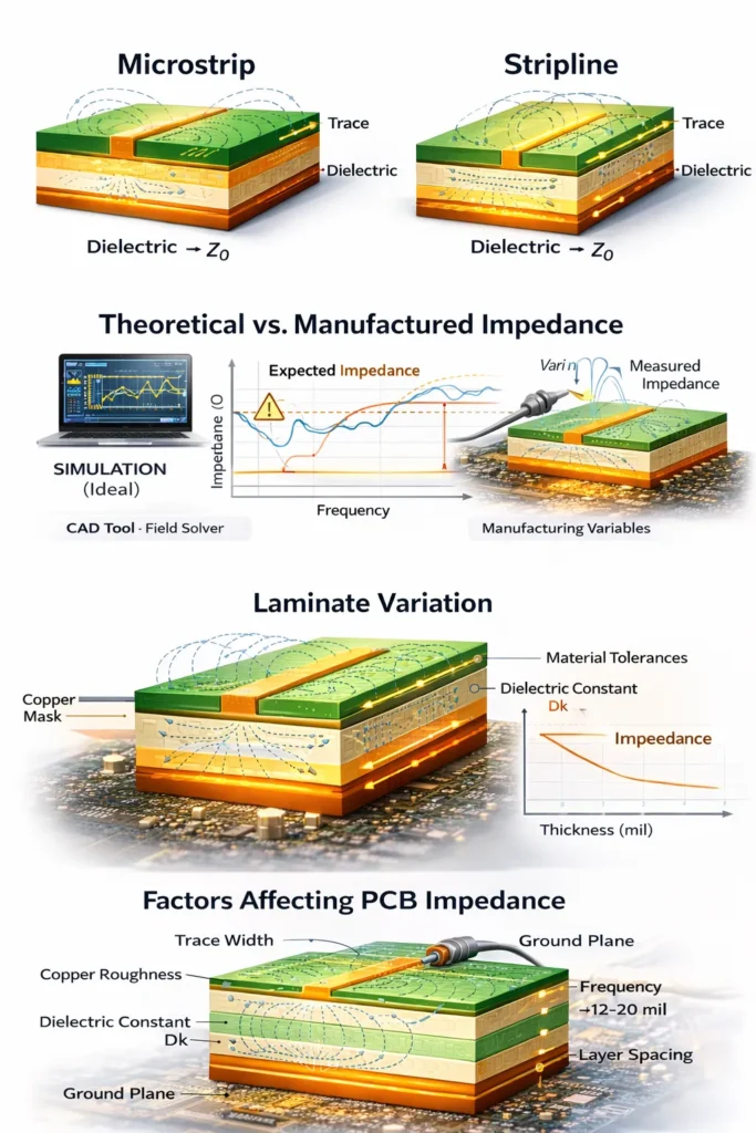
The first reason is the difference between theoretical impedance and manufactured impedance. Most impedance calculations are performed using field solvers or CAD tools based on ideal conditions. These models assume exact material properties, precise copper thickness, and perfect manufacturing processes. In reality, PCB fabrication involves tolerances and material variations that influence the final electrical characteristics of the board.
Laminate variation is one of the most significant factors. PCB laminates are manufactured with a specified dielectric constant (Dk), but that value can vary slightly from batch to batch. Even small differences in Dk can change the impedance of a transmission line. Additionally, copper thickness variations during plating processes can alter trace geometry. Thicker copper effectively increases conductor width and changes the electromagnetic field distribution, which directly impacts impedance.
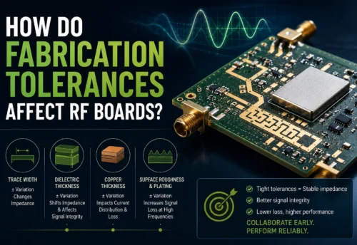
Another common misconception is that trace width alone determines impedance. While trace width is important, impedance is actually influenced by multiple parameters working together. Trace height above the reference plane, dielectric thickness, dielectric constant, copper roughness, and the presence of solder mask all affect signal behavior. Designers who focus only on adjusting trace width often overlook these additional variables that can significantly shift the final impedance value.
The stackup design plays a central role in achieving reliable controlled impedance. The spacing between signal layers and reference planes must be tightly controlled during fabrication. Even small variations in dielectric thickness can change impedance. Because of this, experienced PCB fabricators often adjust trace geometries slightly to compensate for manufacturing realities while still meeting the specified impedance target.
Fabrication tolerances must also be considered. Etching processes can slightly narrow traces, plating processes can add copper thickness, and lamination cycles can compress dielectric layers. Each of these small changes can influence signal performance in high-speed designs.
To improve first-pass success, engineers should include several best practices in their fabrication notes. These include specifying the target impedance and acceptable tolerance, providing the intended stackup structure, identifying reference layers for impedance-controlled traces, and allowing the fabricator to adjust trace width if necessary to meet the impedance specification.
Controlled impedance is not just a design calculation—it is a collaboration between engineering and manufacturing. When designers work closely with experienced PCB fabricators early in the process, the result is a board whose measured performance matches the design intent, ensuring reliable signal integrity in demanding electronic systems.
About Precision PCB
Precision PCB is one of the few true Total Concept providers in the electronics manufacturing industry, delivering both printed circuit board fabrication and full PCBA assembly services under one roof. By offering PCB manufacturing and assembly with a single purchase order, Precision PCB simplifies the supply chain and accelerates product development for engineers and OEMs. Their integrated approach reduces coordination challenges, shortens lead times, and ensures design, fabrication, and assembly work together seamlessly. From prototype to production, Precision PCB provides a complete, end-to-end electronics manufacturing solution that helps customers move from concept to finished product faster and more efficiently.
For more information go to www.precision4pcb.com or call the president Jay Rupani at 847-439-5447 and he’ll be happy to help you out.
Get Your Controlled Impedance Right the First Time
From stackup design to fabrication tolerances, achieving accurate impedance requires more than calculations. Work with experts who understand real-world manufacturing variables and ensure your board performs exactly as intended.
Expert guidance. Reliable performance. Fast turnaround.
FAQs (Frequently Asked Questions)
What is controlled impedance in PCB design?
Why is controlled impedance important in PCBs?
What factors affect controlled impedance in PCB design?
Several key factors influence impedance:
- Trace width and spacing
- Copper thickness
- Dielectric thickness
- Dielectric constant (Dk)
- Stackup configuration
These parameters must be carefully controlled during both design and manufacturing.
Why does measured impedance differ from calculated impedance?
Measured impedance can differ due to real-world manufacturing variations such as:
- Material (Dk) variation
- Copper plating thickness changes
- Etching and lamination tolerances
These deviations are not fully accounted for in ideal CAD simulations.
Does trace width alone determine PCB impedance?
What role does PCB stackup play in controlled impedance?
What happens if impedance is not properly controlled?
Improper impedance control can lead to:
- Signal reflections
- Data errors
- Timing issues
- Increased EMI and crosstalk
- Reduced overall system reliability
What is the relationship between impedance and signal integrity?
Where can I get controlled impedance PCB manufacturing services in the USA?
Engineers and OEMs in the USA can partner with experienced manufacturers like Precision PCB, who provide controlled impedance design support, stackup validation, and full PCB fabrication and assembly services.