- November 11, 2025
- PCB Assembly, PCB Blog
Lead-Free Soldering in PCB Assembly: Challenges and Solutions
In recent years, the electronics manufacturing industry has undergone a significant transformation driven by environmental regulations and increasing awareness of health and sustainability issues. Central to this transformation is the shift from traditional lead-based solder to lead-free alternatives – especially in PCB (Printed Circuit Board) assembly. For a company like Precision4PCB that serves global markets, embracing lead-free soldering isn’t just environmentally responsible – it’s practically mandatory for regulatory compliance and future-proofing.
This post dives deep into the why, how, the challenges, and the practical solutions for lead-free soldering, with a focus on complying with RoHS (Restriction of Hazardous Substances) and selecting suitable solder alloys and processes.
What is RoHS – And Why It Matters
- RoHS is a regulatory directive initially introduced by the European Union to limit hazardous substances in electronic and electrical equipment (EEE). The list of restricted substances includes lead (Pb), mercury, cadmium, hexavalent chromium, certain flame retardants, and more.
- For a PCB assembly to be considered RoHS-compliant (and thus acceptable for sale in many global markets), the lead content in homogeneous materials must typically stay below 0.1% by weight.
- This restriction has driven the widespread adoption of lead-free solder – solder alloys formulated without lead (or with trace amounts well below regulatory limits).
Why it matters for Precision4PCB and customers:
- Ensures compliance with global export regulations (EU, and many other regions follow RoHS or similar rules)
- Demonstrates commitment to environmental responsibility and occupational safety (reducing lead exposure for workers)
- Improves recyclability and disposal safety of electronic products – important in a world increasingly concerned with e-waste.
Common Lead-Free Solder Alloys & Their Properties
Not all lead-free solders are the same. The choice of solder alloy depends on application, cost, thermal and mechanical demands, and board design considerations. Some of the widely used lead-free alloys include:
| Alloy / Composition | Typical Use / Advantages |
|---|---|
| Sn-Ag-Cu (SAC) (e.g. SAC305) - ~95% tin, ~3–4% silver, ~0.5–0.7% copper | Industry-standard for general PCB assembly: good thermal/mechanical properties; reliable solder joints. |
| Tin-Copper (Sn–Cu) | More cost-effective lead-free option, often used where budget matters and high-end mechanical strength is less critical. |
| Other specialized alloys (e.g. with bismuth, tin-zinc, etc.) | Used for specific applications - e.g. when lower melting point or special thermal/mechanical properties are required. |
Lead-free solder alloys have become the backbone of RoHS-compliant PCB manufacturing.
Challenges of Lead-Free Soldering in PCB Assembly
Switching from traditional tin-lead solder to lead-free alloys brings several technical and operational challenges. Understanding these is crucial for implementing reliable, high-quality lead-free assembly processes.
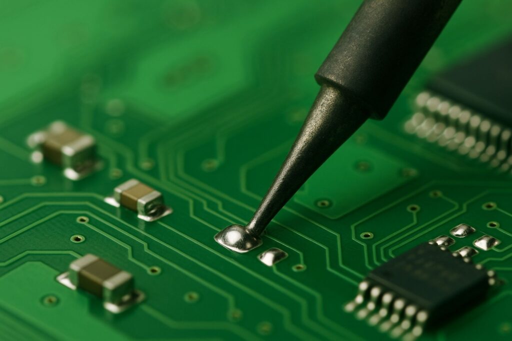
1. Higher Melting and Reflow Temperatures
- Lead-free solders melt at significantly higher temperatures – commonly around 217 °C (or even higher depending on alloy) vs ~183 °C for lead-based solder.
- This increased thermal requirement can stress PCBs, components, and soldering equipment. In some cases, it may result in deformation, delamination, or damage – especially for boards or components not designed for high-temperature assembly.
- Rework becomes more difficult: soldering iron tips wear faster due to higher heat, and fluxes may degrade or burn if not specified for lead-free processes.
2. Poorer Wettability and Flow Behavior
- Lead-free solder generally exhibits worse wettability compared to lead-based solder – meaning it doesn’t flow and spread as readily during soldering/reflow.
- As a result, solder joints may suffer from defects: incomplete fillets, voids, inconsistent bonding, or “cold solder” joints.
- This can lead to lower joint reliability, especially under thermal cycling, vibration, or mechanical stress.
3. Reliability Concerns – Thermal Fatigue, Joint Cracking, Long-term Stability
- Due to different mechanical properties (less ductility, different thermal expansion behavior), lead-free solder joints may be more susceptible to thermal fatigue, cracking, or failure over time – particularly in harsh environments or where boards undergo many thermal cycles.
- Surface finishes and components must be compatible: not just the solder alloy, but also PCB surface finish, via plating, component leads, and flux must be qualified for lead-free assembly.
- For some high-reliability or high-frequency applications, signal integrity, mechanical stress, or environmental conditions may present additional challenges.
4. Increased Cost and Process Overheads
- Lead-free solder alloys tend to be more expensive – more tin, silver, copper, or other metals; this increases material cost.
- Energy costs go up because higher reflow temperatures consume more power and may require more carefully controlled thermal profiles.
- Rewriting process parameters, retraining staff, qualifying components and materials, and performing reliability testing adds overhead – especially relevant for companies switching existing lead-based workflows.
Practical Solutions for Reliable Lead-Free PCB Assembly
Despite the challenges, many of them can be effectively mitigated – and many manufacturers (including those aiming at RoHS-compliance) succeed in producing high-quality, reliable lead-free PCBs. Here are some best practices and solutions:
Use of Industry-Proven Alloys (e.g. SAC) & Proper BOM Control
- Adopt standard lead-free alloys such as SAC (Sn-Ag-Cu) which have well-characterized thermal/mechanical properties and broad industry acceptance.
- Maintain strict control of BOM (Bill of Materials): ensure components, surface finishes, PCB finish, fluxes etc. are all lead-free and compatible with higher reflow temperatures.
Reflow / Soldering Profile Optimization & Equipment Upgrades
- Update reflow oven profiles to account for the higher melting point of lead-free solder; ensure PCB laminates and components can safely handle the thermal load.
- Use soldering irons and tips designed for lead-free processes (higher wattage, better heat transfer, resistant to oxidation). Regular tip tinning helps extend tip life.
- Employ fluxes and solder pastes formulated for lead-free soldering, and ensure proper post-solder cleaning to remove flux residues that might cause corrosion or electrical issues.
PCB Design and Material Considerations
- Use laminates and PCB materials rated for the higher thermal budgets of lead-free assembly – to avoid warping, delamination, or substrate damage.
- For fine-pitch, high-density, high-frequency or high-reliability boards, pay extra attention to pad/via design, thermal stress mitigation, and ensure solderability (footprint design, pad finish, soldermask, etc.) is compatible with lead-free soldering.
- Where needed, consider alternate surface finishes such as lead-free HASL, ENIG, Immersion Silver/OSP – depending on application and component compatability.
Comprehensive Process Qualification, Testing & Quality Control
- Before full production, validate lead-free soldering process via prototype runs and reliability testing (thermal cycling, mechanical stress tests, inspection of solder joints, etc.) to ensure long-term performance.
- Use appropriate inspection techniques to detect soldering defects – voids, insufficient fillet, poor wetting, cold joints, bridging, etc. Implement rework or redesign if necessary.
- Maintain documentation and traceability for all materials and processes – which is essential not only for quality but also for regulatory compliance and customer trust.
Why Precision4PCB Should Embrace Lead-Free PCB Assembly (Especially for Global Clients)
1. Regulatory Compliance & Market Access: With RoHS (and similar regulations globally) being a standard requirement, lead-free assembly ensures that PCBs and devices meet necessary environmental and safety standards – enabling export to EU, North America, and other regulated markets.
2. Environmental Responsibility & Corporate Sustainability: Reducing toxic lead content aligns with global sustainability goals and improves company image among environmentally conscious customers.
3. Safety for Workers & End Users: Eliminates lead exposure risks for manufacturing personnel and reduces harmful waste in e-waste disposal.
4. Future-Proofing & Global Competitiveness: As traditional leaded solder becomes increasingly restricted, lead-free processes ensure that Precision4PCB remains a competitive, compliant, forward-looking PCB manufacturer.
5. Cost of Non-Compliance: Failure to comply can lead to regulatory rejection, increased costs of rework/redesign, or restricted market access – in many cases far costlier than initial investments in lead-free capabilities.
Frequently Asked Questions (FAQ)
Lead-free solder is an alloy that does not use lead (Pb) or keeps it below regulated trace limits. Common lead-free alloys use tin (Sn) as base metal, often with silver (Ag) and copper (Cu) – e.g. Sn-Ag-Cu (SAC).
Yes – when properly implemented. Lead-free solders like SAC can provide reliable mechanical and thermal performance. However, they demand careful control of soldering temperature, PCB materials, solder paste, and process parameters. Improper implementation can lead to inferior joints or reliability issues.
Typically, yes. Lead-free solder alloys are more expensive, require higher energy input (for higher reflow temperatures), and often require equipment/process upgrades and staff training. These all contribute to increased cost.
There can be – especially if the soldering process is not optimized. Potential issues include poor wetting, solder joint cracking under thermal cycling, PCB warping, or component stress. But with proper materials, process controls, and qualification, these risks can be mitigated.
Surface finishes such as lead-free HASL, ENIG (Electroless Nickel Immersion Gold), Immersion Silver, OSP (Organic Solderability Preservative), among others, are commonly used. These finishes, along with solder paste and component terminations, must all comply with lead-free / RoHS standards.
For any product intended for global markets (especially EU, North America, parts of Asia). Also, for manufacturers aiming for sustainable, environmentally friendly practices – and for customers who care about recyclability and long-term product safety. It’s especially relevant for consumer electronics, industrial electronics, IoT devices, and any electronics subject to regulations or environmental standards.
Conclusion & Recommendation
Transitioning to lead-free soldering is no longer optional – for any modern PCB manufacturer aiming at global compliance and sustainability. While the move introduces some technical challenges (higher temperatures, solderability issues, increased cost), these are well understood by the industry – and there are established solutions and best practices to mitigate risks.
For a company like Precision4PCB, embracing lead-free soldering (with properly selected alloys, qualified materials, and optimized processes) offers a win-win: regulatory compliance and global market access, plus environmental responsibility and safer manufacturing.