- November 4, 2025
- PCB Blog, PCB Manufacturing
A Guide to PCB Manufacturing Tolerances and Standards
Designing and manufacturing a reliable printed circuit board (PCB) isn’t just about getting the circuit right – it’s also about respecting the tight tolerances and standards that govern every dimension, clearance, and copper feature on the board. Whether you’re a seasoned PCB designer or new to PCB fabrication, understanding these constraints helps you hit right-first-time manufacturing, reduce scrap, and maintain quality.
In this post we’ll cover the key standards from IPC, what they mean for drill-hole tolerances, trace width and spacing, and other critical manufacturing constraints.
Why Manufacturing Tolerances Matter
- Real-world variation is inevitable. Even the most precise drilling and etching machines deviate slightly – materials shift, copper etches unevenly, drills wander, and plating adds copper where you didn’t draw it.
- Tolerance defines acceptability. Instead of expecting a perfect match to the design, tolerances define acceptable upper and lower bounds. Variations within those bounds should not affect PCB performance.
- Standards enable interoperability and quality control. By adhering to standard tolerances, both designers and manufacturers speak the same “language,” reducing errors and issues in procurement, fabrication, and assembly.
Failing to account for tolerances may result in misaligned holes, insufficient annular rings, poor solderability, unreliable trace integrity, or even total board failure.
Key IPC Standards for Designers & Manufacturers
Overview of Core IPC Standards
- IPC-2221 – the generic standard for PCB design. It defines the fundamental design rules (clearance, spacing, conductor geometry, high-voltage spacing, dielectric selection, etc.) that apply to most rigid and flex PCBs.
- IPC-2152 – provides more detailed guidance (than IPC-2221) for trace current-carrying capacity, thermal performance, and optimized conductor sizing.
- IPC-6012 – the acceptance/performance standard for rigid PCBs, defining manufacturability and acceptance criteria (drill accuracy, copper features, annular rings, plating, etc.).
- IPC-A-600 – complementary to IPC-6012, providing visual criteria (photos/illustrations) of acceptable and unacceptable boards, useful for inspection and quality control.
Depending on the application (consumer electronics vs. medical/military vs. high-voltage), you might pick different “classes” or levels of rigor under IPC standards.
Drill Hole & Via Tolerances
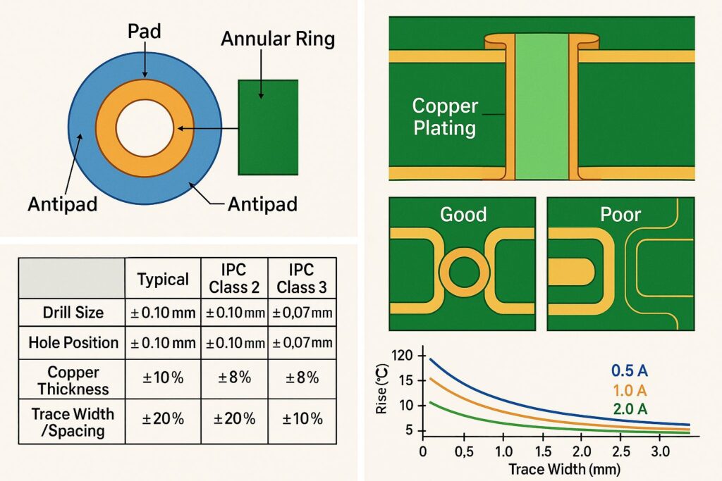
Drill Size, Hole Position & Plating
- According to typical industry practice, plated-through hole (PTH) diameters (≤ 4.00 mm) often carry tolerances around ±0.10 mm; for holes larger than 4.00 mm, tolerance may widen to ± 0.20 mm.
- Some more precise shops and boards may aim for tighter tolerance, e.g. ±0.05 mm for plated holes.
- Hole-to-hole position (pattern tolerance) also has limits. Some references cite typical positional tolerances around ±0.10 mm for general hole patterns.
Annular Rings & Pad Sizing
- For PTH / via pads: the pad must be larger than the hole to ensure an annular ring (the copper ring around the hole). Standard guidance: pad size = finished hole size + 2 × (minimum annular ring) + fabrication allowance.
- For example (for 1/2 oz copper, typical for many boards under class-3): a 0.008″ drill might have a pad of 0.023″, with an antipad (clearance ring on adjacent plane) of 0.033″.
- For high-reliability boards (class 3), lifted or fractured annular rings and drill breakouts are not acceptable.
Copper Plating Thickness
- The base-copper thickness itself is subject to manufacturing variation. Under IPC-4562 (which defines raw copper base material specs), it’s common to allow up to a 10% reduction from nominal base copper thickness.
- This is important because trace current carrying capacity and plating requirements depend on actual copper thickness – not just the nominal value.
Trace Width, Spacing & Thermal / Current Considerations
Standards and Their Role
- The IPC-2221 standard provides baseline guidance for conductor geometry, spacing, and clearance, including spacing for high-voltage boards.
- For current-carrying traces, thermal rise, and reliability, IPC-2152 offers more refined guidance compared to IPC-2221. It accounts for copper weight, board stack-up, presence of copper planes, thermal environment, etc.
Typical Manufacturing Tolerances on Trace Width & Spacing
- In many fabrication shops, trace width and spacing can vary by ±10% to ±20% from the targeted design dimension depending on process, copper thickness, and board complexity.
- Some sources mention a more conservative tolerance like ±0.005 inches (~±0.127 mm) for trace width in certain process flows.
- For tight-tolerance, high-density or high-reliability boards (e.g. class 3), manufacturers may impose stricter constraints on minimum trace width, spacing, and conductor spacing from board edges or between copper features.
Electrical and Thermal Performance
- The width (and thickness) of a trace determines how much current it can safely carry without excessive heating. Using IPC-2221 (and more accurately IPC-2152) trace-width calculators helps estimate required conductor size for a given current and acceptable temperature rise.
- Because IPC-2221’s rules are conservative (especially regarding thermal rise in worst-case conditions), many modern designs using copper pours, planes, or controlled impedance layers may safely deviate – but only if well-analyzed.
Board Edge, Clearance & Other Mechanical Tolerances
- It’s common to hold copper features (traces, pours) a minimum distance away from the board edge – for example, many fabricators recommend at least 0.020 inches (≈ 0.5 mm) of clearance between copper and board edge.
- For drilled holes near the board edge, maintain a buffer: at least 0.020 inches from board edge, and more if the board will be separated from a panel (e.g. via V-groove or breakout tabs).
- Because of all the cumulative tolerances (hole location, plating, etch, copper shift), what you draw in CAD will almost never be exactly what you get – which is why adhering to IPC clearance, spacing, and pad-to-edge rules is critical.
IPC Classes: What They Mean for Tolerance & Acceptability
The IPC standards define different “classes” of boards – and the class determines how strict tolerances, inspection, and acceptance criteria are.
- Class 1 – for basic consumer electronics, simple functionality, lower reliability and shorter lifespan. Cosmetic defects are often acceptable.
- Class 2 – for dedicated electronic products requiring moderate reliability (e.g. home appliances, computers, general industrial). Allows some minor cosmetic imperfections but requires standard engineering tolerances.
- Class 3 – for high-reliability, mission-critical boards: medical, aerospace, automotive safety, military, etc. Requires much tighter control over tolerances, no lifted/fractured annular rings, stricter trace/pad/spacer rules, and more rigorous inspection (e.g. visual, AOI, X-ray).
For a manufacturing partner like Precision4PCB, it’s essential when quoting jobs to know what “class” the customer’s design must meet – this directly affects allowable tolerances, cost, yield, and inspection effort.
Putting It All Together: Designing for Manufacturability
Here are practical design-for-manufacturing (DFM) guidelines to make your board more “fab friendly” and reduce iteration cycles:
- Define the Class up front – Before routing or placing vias, know whether your board is Class 2 or Class 3 (or higher) depending on the application.
- Pad and Via Planning – Always size pads larger than finished hole diameter sufficiently to guarantee a reliable annular ring. Use standard pad-to-hole rules (hole + 2 × minimum annular ring + fabrication allowance).
- Allow Clearance to Edges – Keep copper & holes a safe distance from board edges (e.g. ≥ 0.020″). If board will be routed out or depanelized, leave extra buffer.
- Be Conservative with Trace Width/Spacing – While modern processes may allow aggressive trace/space, keep design within standard tolerances (±10-20%) unless you coordinate with the fab house.
- Use IPC Trace Calculators for Current-Carrying Traces – For power nets or high-current traces, use IPC-2221 / IPC-2152 calculators to derive minimum safe trace width (given copper thickness, current, temperature rise allowance).
- Communicate with Your Manufacturer – Provide clear drawings and specify whether you need Class 2 or Class 3 acceptance. Get confirmation about minimum copper weight, plating spec, drill tolerances, and inspection criteria.
- Anticipate Variation & Inspect Early – Order a test batch or prototype if your design is tight or high-reliability; get cross-sections or AOI reports to verify annular rings, plating, and trace integrity before mass production.
Frequently Asked Questions (FAQ)
For very small holes (micro-vias), tolerances become more challenging. Pads must still offer enough annular ring, and plating must be carefully controlled. You should consult with your fabricator early, and often micro-vias may require laser drilling, controlled dielectric thickness, and special plating – potentially beyond standard IPC-6012 rigid-PCB specs.
Use IPC-2221 as a baseline – it’s generic and widely accepted. For more accurate current/thermal calculations (especially for power nets), IPC-2152 is preferred because it accounts for real-world factors like copper weight, copper planes, and board stack-up.
As a rule of thumb, leave at least 0.020″ (~0.5 mm) between copper and board edge. For boards to be depanelized (e.g. via V-groove or tabs), give extra margin. This reduces risk of copper lift, edge defects, or mechanical stress during routing and handling.
Conclusion
Understanding and designing to manufacturing tolerances and standards is just as critical as getting your circuit schematic right. By aligning your designs with the guidance of IPC standards (like IPC-2221, IPC-2152, IPC-6012, and IPC-A-600), you significantly improve your chances of first-pass success, reduce manufacturing risk, and increase board reliability – especially important when you’re building high-quality products such as those manufactured at Precision4PCB.
Whether you’re designing a simple consumer-level board or a high-reliability board for critical applications, integrating DFM thinking early saves time, cost, and rework.
Get an Instant PCB Manufacturing Quote.