
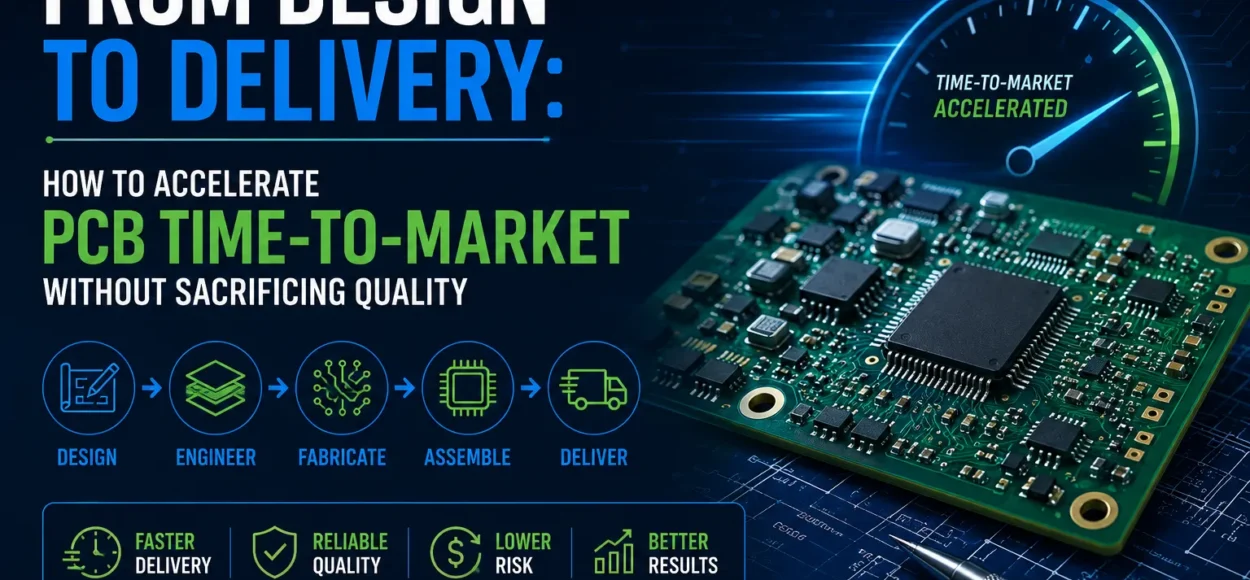
From Design to Delivery: How to Accelerate PCB Time-to-Market Without Sacrificing Quality
You already know speed matters. But let’s go deeper—because if you’re an engineer, you don’t care about slogans. You care about what actually works. This is where most articles fall apart. They talk about speed in general terms. What you need is specifics—the technical decisions, process improvements, and engineering discipline […]

The True Cost of Cheap PCBs: What No One Tells You
Core Question: Why are low-cost PCB quotes often misleading? Let’s start with a hard truth. If you’re choosing a PCB supplier based on price alone, you’re not saving money. You’re placing a bet. And more often than not, it’s a bad one. Because the cheapest quote on the table is […]

What Engineers Really Look for in a PCB Manufacturing Partner
Engineers don’t choose PCB suppliers the way purchasing departments think they do. They don’t sit around comparing spreadsheets, arguing over pennies per board, or obsessing over who shaved half a day off a standard lead time. That’s not how real decisions get made—at least not the ones that matter. Engineers […]

The Total Concept Advantage: Why One Partner Beats Five Vendors Every Time
There’s a moment in almost every electronics project when things start to feel… harder than they should be. The design is solid. The idea is right. The market is ready. And yet, progress slows. Emails multiply. Questions go unanswered. Timelines stretch. Small issues turn into big ones. And suddenly, instead […]
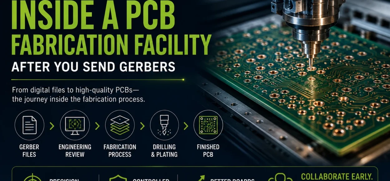
What Happens Inside a PCB Fabrication Facility After You Send Gerbers
When engineers release Gerber files for a printed circuit board, the design often feels complete. In reality, that is when the manufacturing journey begins. Inside a PCB fabrication facility, a series of precise and tightly controlled processes transform those digital files into a physical circuit board. Understanding what happens during […]
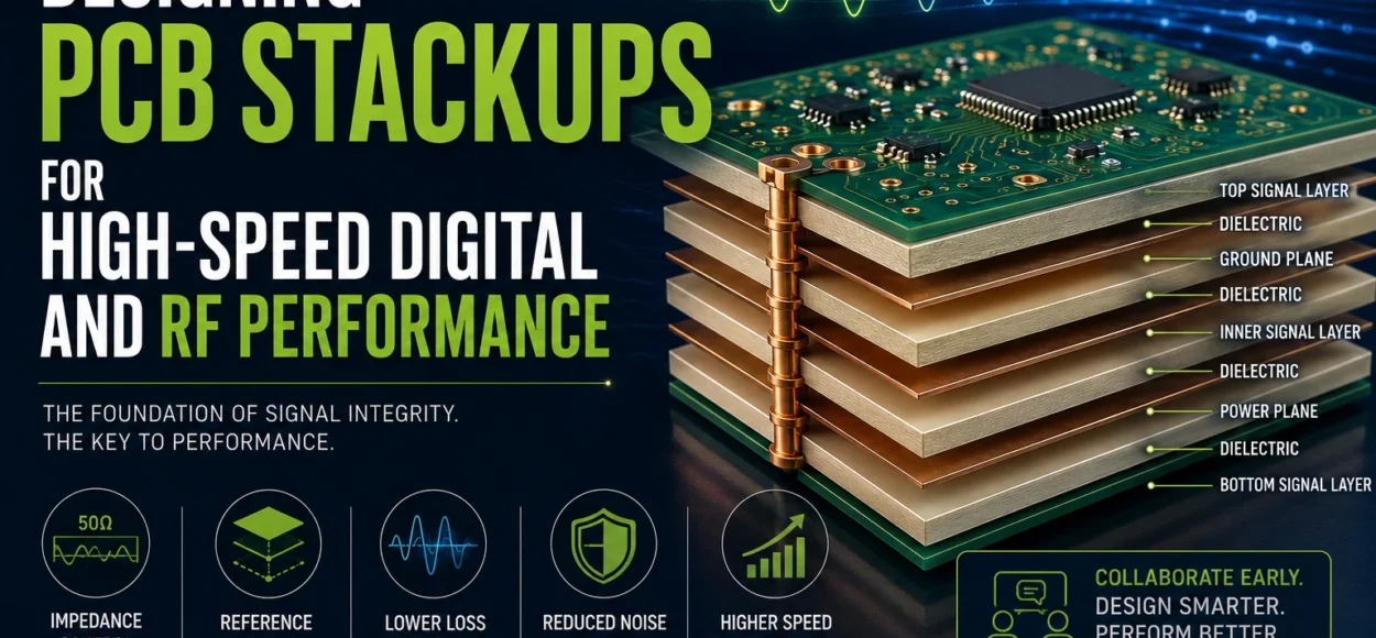
Designing PCB Stackups for High-Speed Digital and RF Performance
As digital speeds climb into multi-gigabit territory and RF designs push deeper into microwave frequencies, PCB stackup design has become one of the most critical elements of successful electronic systems. While many engineers focus primarily on routing and component placement, the truth is that signal integrity is often determined long […]
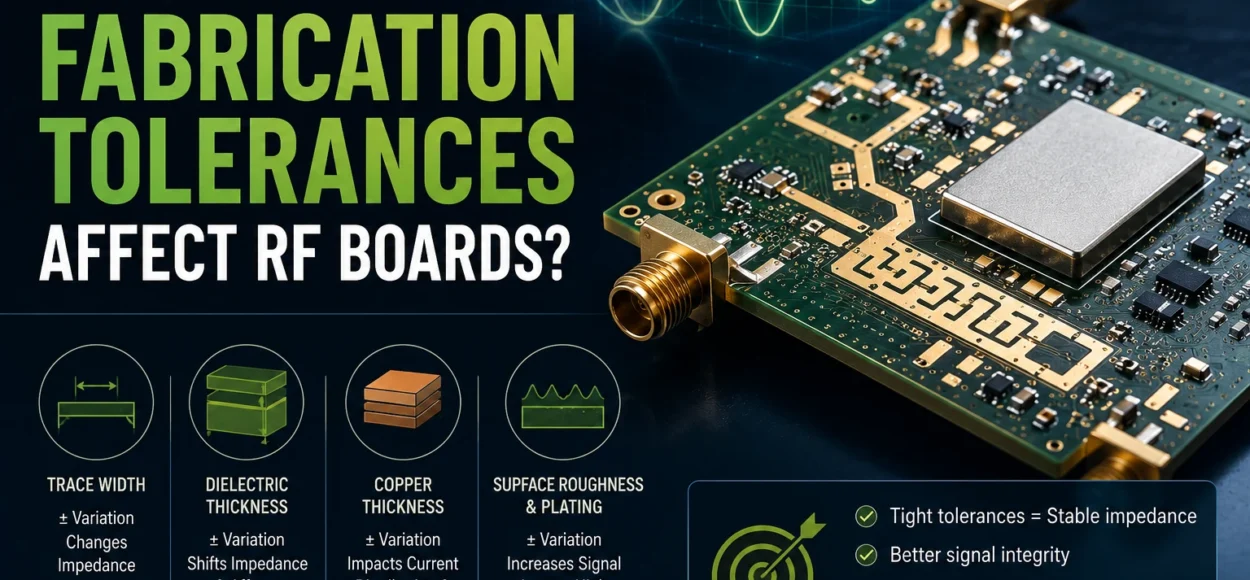
How Do Fabrication Tolerances Affect RF Boards?
RF circuit performance depends heavily on precise physical geometry, which means fabrication tolerances play a major role in how the finished board performs. Parameters such as trace width, dielectric thickness, copper thickness, and laminate consistency directly influence impedance and signal loss. Even small variations in these parameters can shift impedance […]
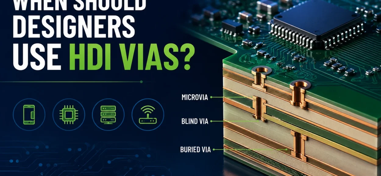
When Should Designers Use HDI Vias
High Density Interconnect (HDI) vias are most useful when circuit designs require extremely dense component layouts or advanced packaging technologies. As electronics become smaller and more powerful, traditional through-hole vias often limit routing flexibility. HDI structures use microvias, blind vias, and buried vias to connect layers without consuming large amounts […]
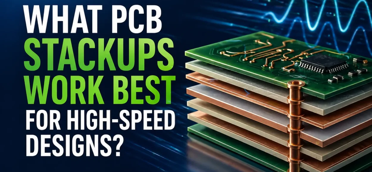
What PCB Stackups Work Best for High-Speed Designs?
High-speed digital circuits depend heavily on the PCB stackup structure, because the stackup determines impedance control, signal integrity, and electromagnetic performance. Most high-speed designs perform best with symmetrical multilayer stackups that include dedicated reference planes. A common configuration is a 6-layer or 8-layer stackup with signal layers adjacent to solid […]

What Are the Advantages of a Total Concept PCB Partner (Fabrication and Assembly)?
A Total Concept PCB provider offers both PCB fabrication and PCB assembly from a single source, giving engineers a more efficient and reliable path from design to finished electronics. Instead of coordinating between multiple vendors, designers work with one technical team that understands the entire manufacturing process. This integrated approach […]