PCB Prototyping: From Design to First Batch Production
A Step-by-Step Guide to Turning Your Circuit Design into Reality
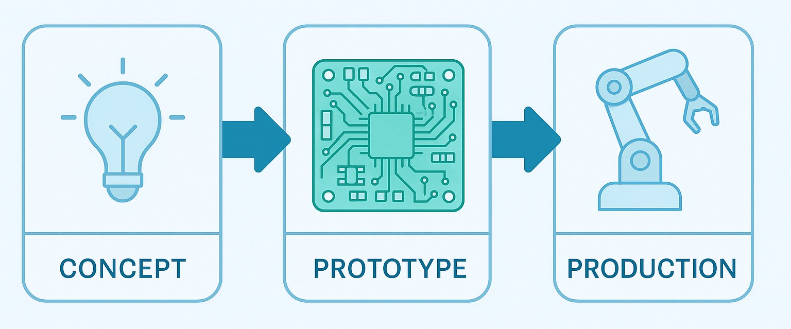
In today’s fast-paced electronics industry, PCB prototyping is the crucial bridge between concept and production. Whether you’re designing an IoT device, medical sensor, or industrial controller, a well-executed prototype ensures functionality, reliability, and manufacturability – before investing in full-scale production.
At Precision4PCB, we specialize in rapid PCB prototyping and low-volume production, helping engineers and innovators transform their designs into high-quality boards – efficiently and cost-effectively.
This guide walks you through every step of the PCB prototyping process, from schematic design to your first production batch.
Table of Contents
What Is PCB Prototyping?
Step 1: Schematic Design and Component Selection
Step 2: PCB Layout Design
Step 3: Design Rule Check (DRC) and Gerber File Preparation
Step 4: PCB Fabrication
Step 5: PCB Assembly (SMT/THT)
Step 6: Testing and Quality Assurance
Step 7: Design Validation and Iteration
Step 8: Transition to First Batch Production
Precision4PCB’s Prototyping Advantage
FAQs
Conclusion
What Is PCB Prototyping?
PCB prototyping is the process of creating a working version of your printed circuit board before mass production. It validates both electrical performance and mechanical fit.
The goal is to identify design flaws, signal issues, or layout inefficiencies early – saving both time and cost down the road.
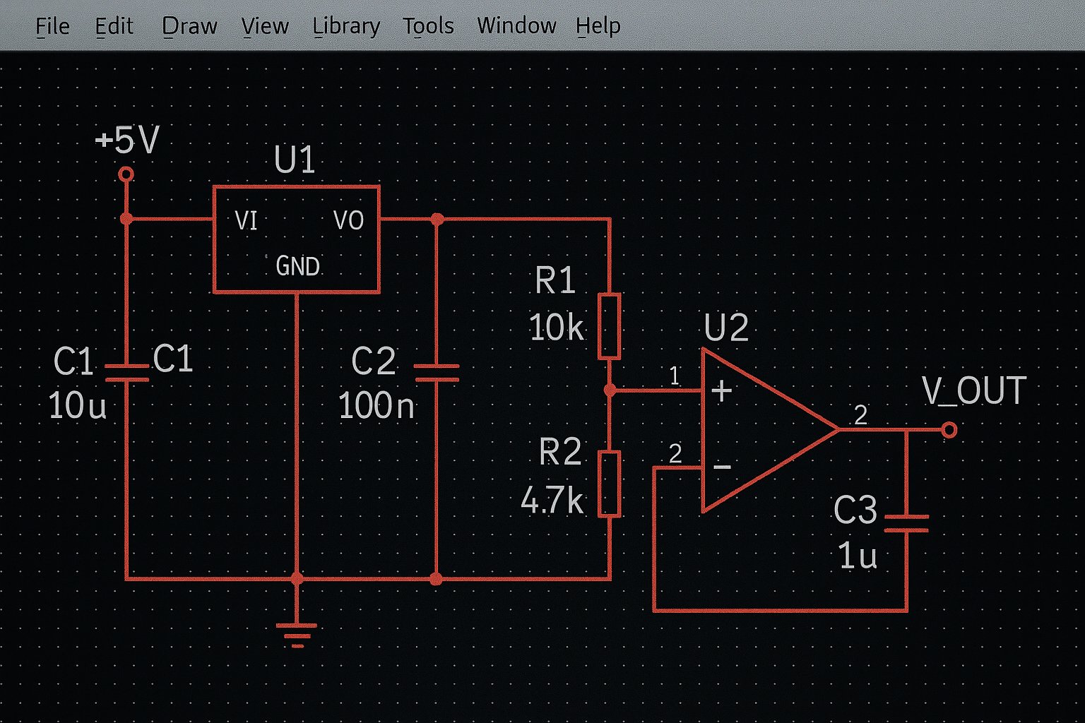
Step 1: Schematic Design and Component Selection
Every PCB begins with a schematic – a digital map of all electronic connections.
In this phase:
Engineers draw the circuit diagram using software like Altium Designer, KiCad, or OrCAD.
They select components such as ICs, resistors, capacitors, and connectors based on electrical needs and availability.
Best Practices:
Choose components from trusted distributors to avoid counterfeit parts.
Consider footprint compatibility with manufacturing standards.
Keep BOM (Bill of Materials) organized for sourcing efficiency.
Step 2: PCB Layout Design
Once the schematic is finalized, it’s converted into a layout – the physical design of copper traces and component placement on the board.
This step determines:
Trace width and spacing
Via placement and routing
Layer count (single, double, or multilayer)
Ground and power planes
At Precision4PCB, our engineers optimize layouts for:
Signal integrity
Thermal management
Electromagnetic compatibility (EMC)
Step 3: Design Rule Check (DRC) and Gerber File Preparation
Before sending a design to production, engineers perform a Design Rule Check (DRC) to ensure compliance with fabrication tolerances.
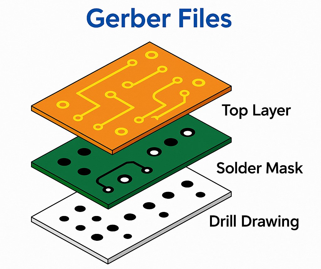
Once verified, the design is exported into Gerber files – the industry-standard format that defines:
Copper layers
Solder mask
Silkscreen
Drill holes
These files serve as the blueprint for manufacturing.
Tip: Always include a readme file specifying stack-up details and any special manufacturing requirements.
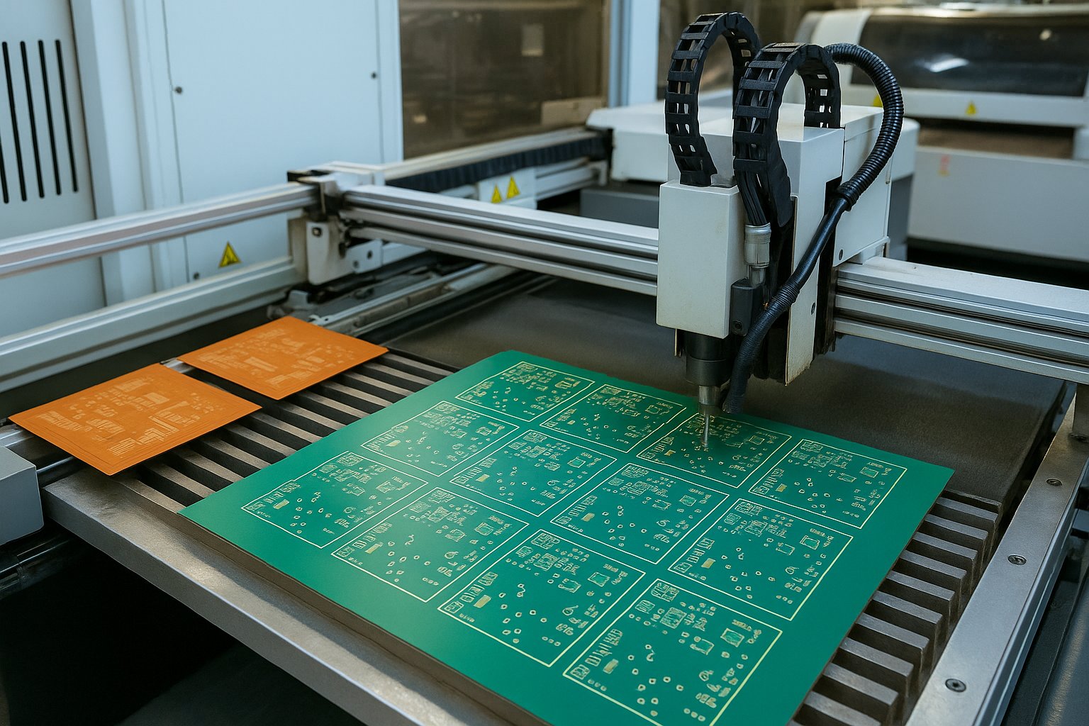
Step 4: PCB Fabrication
This is where your design becomes tangible. PCB fabrication involves multiple processes:
Copper Cladding: Applying conductive copper sheets to the substrate.
Photoresist Imaging: Transferring the PCB pattern using UV exposure.
Etching: Removing excess copper to reveal the circuit traces.
Drilling: Creating holes for vias and through-hole components.
Solder Mask & Silkscreen: Protecting circuits and labeling parts.
Precision4PCB uses advanced CNC and laser systems to ensure tight tolerances and high precision even for fine-pitch components.
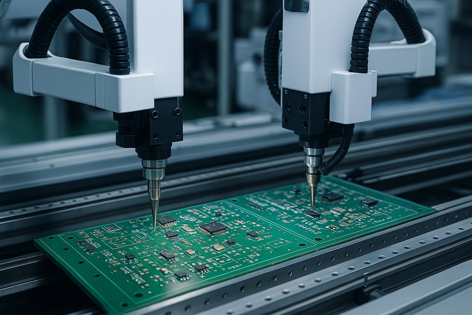
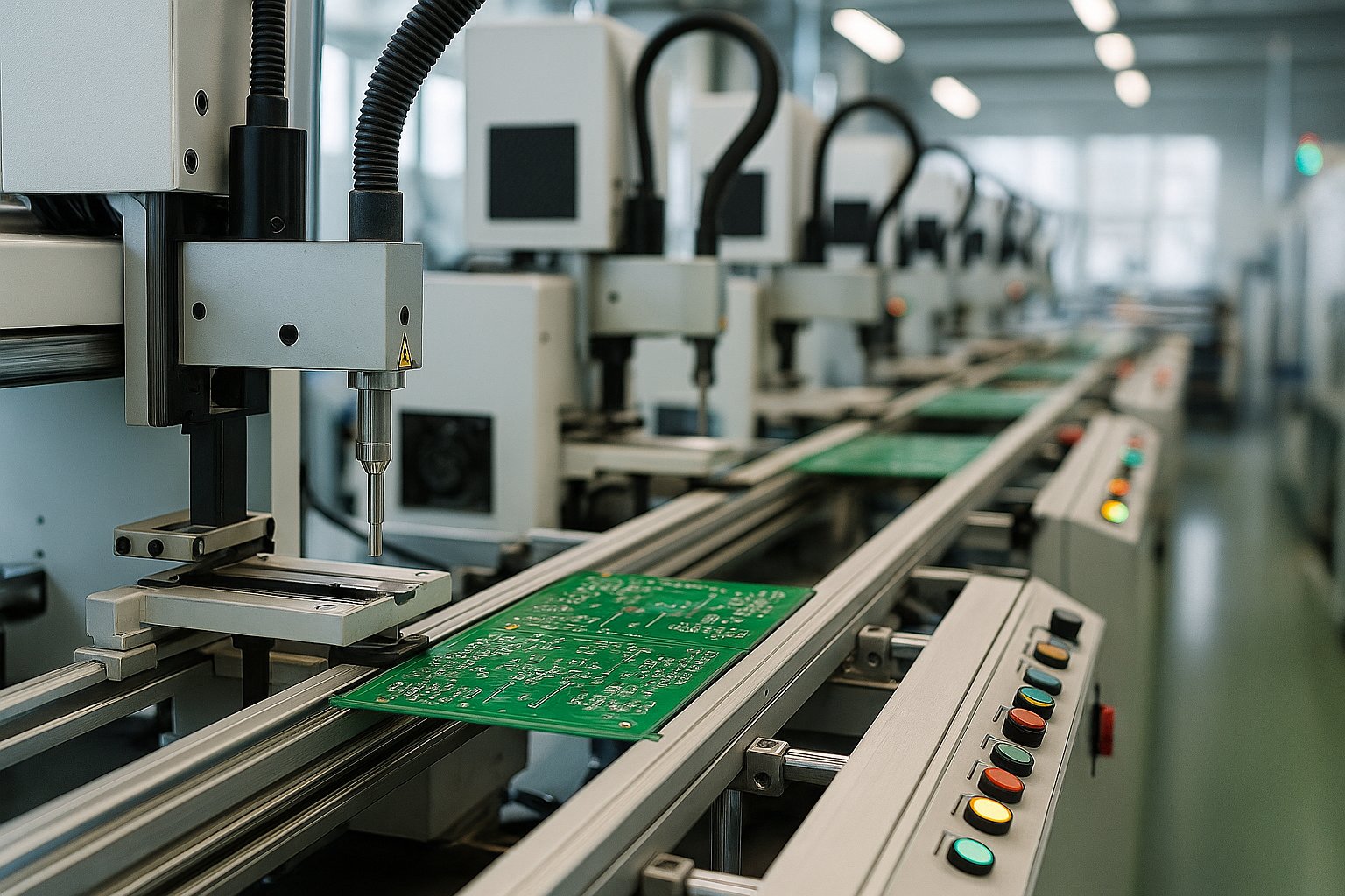
Step 5: PCB Assembly (SMT/THT)
After fabrication, the boards move to assembly, where components are mounted.
Two main techniques are used:
SMT (Surface Mount Technology): Components are soldered directly onto the surface.
THT (Through-Hole Technology): Leads are inserted into drilled holes and soldered.
The process includes:
Solder paste printing
Pick-and-place component mounting
Reflow soldering
Manual or wave soldering (for THT)
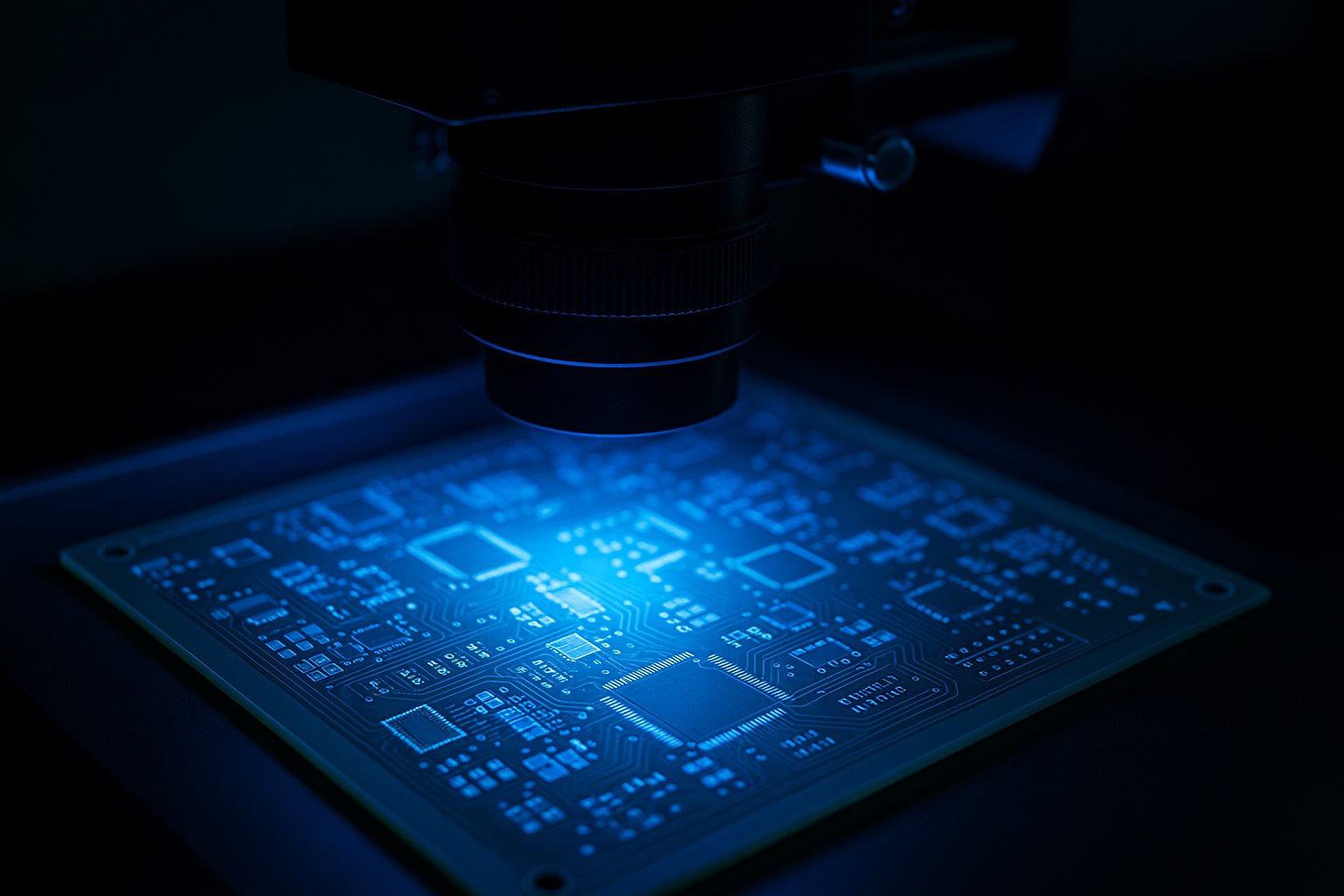
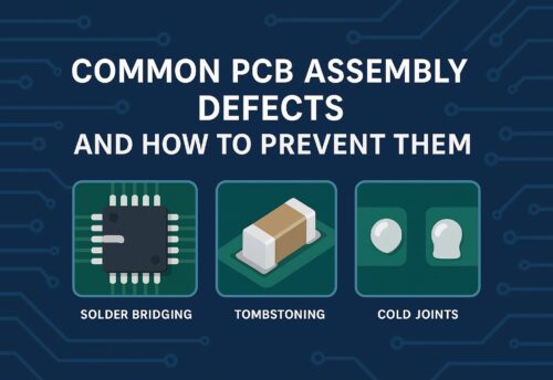
Step 6: Testing and Quality Assurance
Before a prototype is approved, it undergoes multiple tests:
Electrical testing (E-test) for open/short circuits
AOI (Automated Optical Inspection) for solder defects
X-ray inspection for BGA and multilayer issues
Functional testing to verify circuit performance
At Precision4PCB, our inspection systems use AI-based visual analytics to detect even microscopic errors, ensuring each prototype meets client specifications.
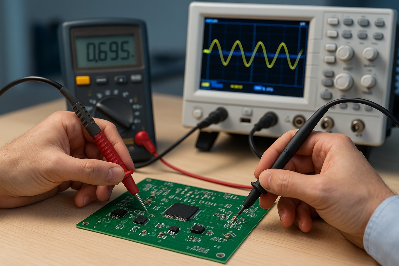
Step 7: Design Validation and Iteration
The prototype is tested under real-world conditions to validate performance.
If any issues arise, engineers analyze test data, update the schematic or layout, and create revised prototypes.
This iterative process ensures the final design is production-ready and optimized for yield, thermal control, and functionality.
Step 8: Transition to First Batch Production
Once validation is complete, the project moves to low-volume batch production.
This stage finalizes:
Manufacturing parameters
Assembly workflow optimization
Supply chain readiness
Precision4PCB ensures the smooth scaling of prototypes to production – maintaining design consistency, component traceability, and cost efficiency.
Precision4PCB’s Prototyping Advantage
At Precision4PCB, we combine experience, precision, and innovation to make prototyping seamless and successful.
Our Services Include:
Rapid prototype fabrication and assembly (1–5 days turnaround)
Support for rigid, flex, and multilayer PCBs
DFM (Design for Manufacturability) review for optimal production
In-house AOI and functional testing
Direct transition to mass production
With cutting-edge manufacturing equipment, AI-driven inspection systems, and expert engineering oversight, we ensure your first prototype is a success – not an experiment.
Conclusion
PCB prototyping is the most critical phase in product development.
By following a structured approach – from schematic to assembly and validation – you can ensure your design is reliable, manufacturable, and cost-efficient.
At Precision4PCB, we bring expertise, technology, and precision to every stage of your prototype journey.
Ready to bring your PCB design to life?
Contact us today to discuss your prototype requirements or request a free design-for-manufacturing (DFM) review.
Prototyping time depends on design complexity. Simple boards may take 2–4 days, while multilayer or high-density boards may require 7–10 days for fabrication and testing.
Prototypes are built to validate functionality, while production PCBs are optimized for volume, yield, and cost efficiency. Prototyping focuses on testing; production focuses on scaling.
Our process includes DFM analysis, AOI and X-ray inspection, and electrical testing. Every prototype is built using IPC class standards to ensure consistent performance.