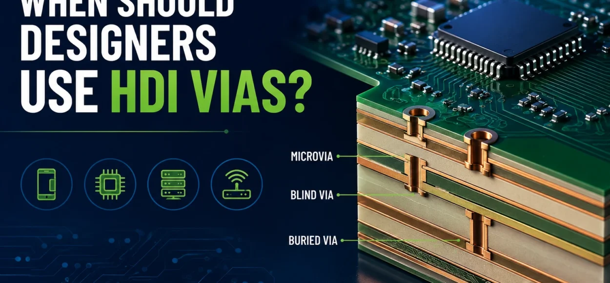
High Density Interconnect (HDI) vias are most useful when circuit designs require extremely dense component layouts or advanced packaging technologies. As electronics become smaller and more powerful, traditional through-hole vias often limit routing flexibility.
HDI structures use microvias, blind vias, and buried vias to connect layers without consuming large amounts of routing space. This allows designers to escape fine-pitch BGAs, reduce layer counts, and achieve higher interconnect density.
Designers typically consider HDI vias when working with 0.5 mm pitch or smaller BGA components, complex mobile electronics, advanced computing devices, and high-performance networking hardware.
Another advantage of HDI is improved electrical performance. Shorter via structures can reduce parasitic inductance and improve signal integrity in high-speed circuits.
However, HDI manufacturing requires specialized fabrication processes such as laser drilling and sequential lamination, so it’s important to consult the PCB fabricator early in the design process. Early collaboration ensures that HDI structures are manufacturable, reliable, and optimized for cost.
Ready to Build High-Density PCBs?
Partner with experienced PCB specialists to bring your HDI designs to life with precision manufacturing and proven reliability.