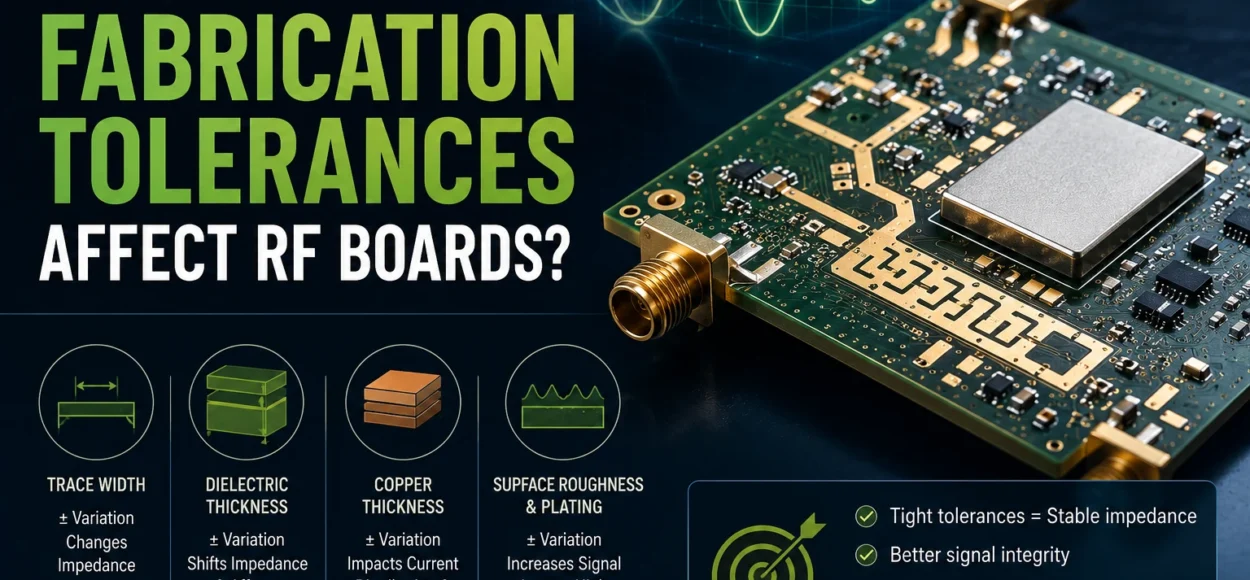
RF circuit performance depends heavily on precise physical geometry, which means fabrication tolerances play a major role in how the finished board performs.
Parameters such as trace width, dielectric thickness, copper thickness, and laminate consistency directly influence impedance and signal loss. Even small variations in these parameters can shift impedance values or change the electrical behavior of RF transmission lines.
For example, a slight change in dielectric thickness can alter impedance enough to degrade signal integrity at microwave frequencies. Similarly, copper surface roughness and plating thickness can increase signal loss in high-frequency applications.
Manufacturers also work within tolerances for etching, drilling, and lamination. These normal manufacturing variations must be considered during design.
The best approach is to involve the PCB fabricator early when developing RF boards. Fabricators can recommend materials, stackups, and design parameters that account for real manufacturing tolerances, helping engineers achieve reliable RF performance on the first build.
Need Precision RF PCB Manufacturing?
Partner with a fabrication team that understands tight tolerances, controlled impedance, and high-frequency design requirements.