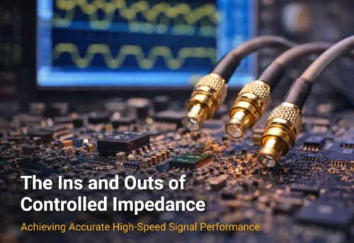
Best Practices for High-Speed PCB Design: How to Mitigate Signal Integrity Issues, Ensure Accurate Impedance Matching, and Optimize Trace Routing
As technology advances, the need for faster, smarter, and more efficient electronic products increases by the day. From next-generation automotive systems and high-end networking gear to consumer devices, high-speed printed circuit boards (PCBs) drive the innovation it all relies on.
But PCB design for high-speed is no longer business as usual. The tactics that succeeded at low frequencies do not work when signals are at gigahertz speeds. Small errors result in signal integrity problems, test failures, and time-consuming redesigns that put time-to-market at risk.
At Precision4PCB , we work with product teams and design engineers who face these challenges every day. In this article, we’re going to take you through best practices in high-speed PCB design and how the appropriate fabrication partner will aid in the prevention of setbacks and achieving first-pass success.
Plan for Signal Integrity from the Beginning

In high-frequency designs, PCB traces behave as transmission lines, not wires. Crosstalk, reflections, and noise can seriously impair performance if they’re not addressed early in the design process.
Best Signal Integrity Practices:
- Identify all high-speed nets (DDR, PCIe, USB 3.0, HDMI, etc.) at the schematic phase.
- Apply signal integrity simulations to detect potential issues before layout and fabrication.
- Work with a PCB manufacturer on stack-up design and dielectric properties to ensure high-speed construction.
At Precision4PCB, our design-for-manufacturing reviews help engineers detect and resolve signal integrity problems before boards go into production.
Impedance Matching is Critical
When impedance is not managed, reflections, timing errors, and signal loss result. In high-speed designs, correct impedance matching is not negotiable.
Impedance Control Best Practices:
- Specify impedance targets early (e.g., 50Ω single-ended, 100Ω differential).
- Calculate trace widths, spacing, and dielectric thickness with accuracy.
- Ensure your fabricator can achieve tight impedance tolerances reliably.
At Precision4PCB, our impedance-controlled fabrication services guarantee that your design intent reaches the finished board.
Smarter Trace Routing for High-Speed Designs
Theory meets reality in routing, and that’s where most designs go wrong. Inadequate routing decisions can cause inductance, reflections, or EMI.
Best Practices for Trace Routing:
- Keep high-speed traces short, straight, and without unnecessary detours.
- Avoid sharp corners and minimize via usage.
- Route differential pairs together with consistent spacing and length matching.
- Isolate noisy signals such as switching regulators from sensitive analog lines.
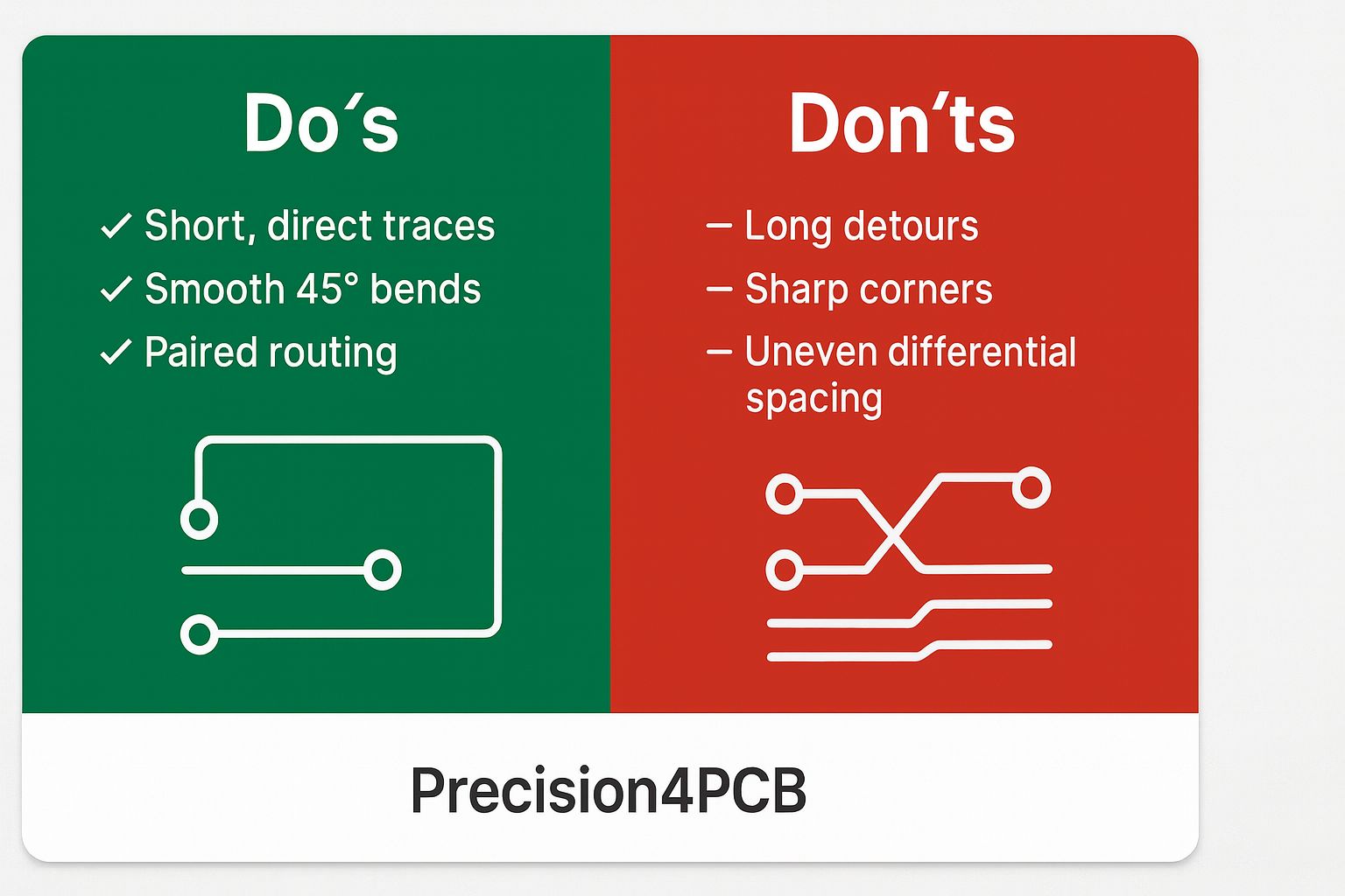
Our cutting-edge fabrication techniques accommodate fine trace/spacing demands, so your routing rules directly map to manufacturing victory.
PCB Stack-Up and Material Selection
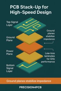
Stack-up determines signal integrity, EMI shielding, and impedance stability. Material selection is just as important at gigahertz frequencies.
Best Practices for Stack-Up & Materials:
- Employ a balanced stack-up with dedicated ground planes.
- Minimize layer transitions for critical high-speed nets
- Select low-loss materials for designs operating at GHz frequencies where standard FR-4 may not be sufficient.
Precision4PCB’s engineers assist with design of custom stack-up and material choice, optimizing between performance and expense.
Choosing the Right Fabrication Partner
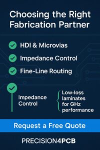
The best PCB layout can fail if the fabrication process cannot hold the tolerances needed for high-speed designs. Selecting the right manufacturing partner is just as important as the design itself.
Best Practices for Partner Selection:
- Work with a fabricator experienced in HDI, microvias, and impedance-controlled builds.
- Verify that they can meet requirements for fine-line routing, consistent dielectric thickness, and advanced laminates.
- Look for a partner who provides end-to-end support, including engineering reviews and quality assurance testing.
At Precision4PCB, we specialize in high-speed PCB fabrication that delivers consistent performance across prototypes and full production runs.
FAQs on High-Speed PCB Design
Q1. What are the greatest challenges in high-speed PCB design?
Most difficult are maintaining signal integrity, impedance control, and routing differential pairs. Stack-up creation and material choice also figure heavily.
Q2. Can FR-4 be applied for high-speed PCB design?
FR-4 is adequate for lower speeds, but at gigahertz frequencies, low-loss laminates (e.g., Rogers, Isola) are much better.
Q3. Why is impedance matching so important?
Signals will reflect back and cause timing errors, data loss, or jitter in high-speed systems if impedance matching is not done correctly.
Q4. In what way do differential pairs assist in high-speed PCBs?
Differential pairs eliminate noise and enhance signal integrity. They maintain tight coupling and length matching to ensure data is transmitted correctly.
Q5. What is the PCB manufacturer’s role in high-speed design?
In addition to fabrication, a seasoned manufacturer assists with stack-up design, impedance modeling, and DFM checks so that your board works as it should.
Final Thoughts
High-speed PCB design is more than tracing – there’s a systems approach: signal integrity, impedance management, trace routing, stack-up strategy, and material selection all count. No less critical is selecting a partner for fabrication who can provide tolerances, materials, and engineering know-how your design calls for.
At Precision4PCB, we integrate engineering assistance, impedance-controlled manufacturing, and quality control to enable you to succeed on the first pass and get your product to market sooner.
Get a Free Quote or Talk to an Engineer today and learn how we can assist in making your high-speed PCB design a success.