
How to Reduce EMI in PCB Design
Practical Tips for Shielding, Grounding, and Stack-Up

As electronic products get faster and more compact, electromagnetic interference (EMI) has become one of the toughest challenges for engineers. EMI can cause devices to behave unpredictably, fail compliance testing, or even disrupt nearby systems. If left unchecked, it often leads to costly redesigns and project delays.
The good news? By planning ahead and using the right design practices, EMI can be greatly reduced. At Precision4PCB, we work with design teams every day to tackle these challenges, and in this guide, we’ll walk through proven strategies you can apply to your next project.
Get Grounding Right
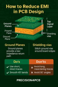
A solid ground system is the backbone of EMI control. Without it, signals have no clean return path, which increases noise and radiated emissions.
Best practices:
- Use a continuous ground plane instead of narrow ground traces.
- Keep return paths short and direct to reduce loop areas.
- Avoid ground loops; stick to single-point grounding or use capacitive coupling where needed.
Plan a Smart PCB Stack-Up
How you layer your PCB plays a huge role in EMI performance.
Tips for stack-up design:
- Place signal layers between power and ground planes for natural shielding.
- Use thin dielectrics between layers so signals stay tightly coupled with their reference plane.
- For multi-layer boards, alternate signal and plane layers to improve shielding and control return currents.
This not only reduces EMI but also improves signal integrity.
Use Shielding and Via Stitching
Sometimes, physical shielding is the best solution.
- A metal enclosure (Faraday cage) around sensitive circuits can block radiated noise.
- Via fencing (a row of closely spaced vias around a trace or PCB edge) creates a mini-shield on the board itself.
These techniques are especially effective in high-frequency designs.
Rethink Your Trace Routing
How you route traces can make or break your EMI performance.
Do’s:
- Keep traces as short and direct as possible.
- Route differential pairs together with consistent spacing.
- Partition the board – keep noisy circuits (like switching regulators) away from sensitive analog sections.
Don’ts:
- Avoid routing traces over splits in ground or power planes.
- Stay away from sharp 90° bends – they increase reflections.
Strengthen Your Power Delivery
Power distribution is often overlooked, but it’s a major EMI source if not managed properly.
- Place decoupling capacitors close to IC pins.
- Use a solid power plane to reduce impedance and noise.
- Think of your power delivery network (PDN) as part of the signal path, not just a background utility.
FAQs About EMI in PCB Design
Q1. Why are ground planes so important?
They provide a low-impedance return path, which keeps loops small and reduces emissions.
Q2. What’s a via fence?
A row of closely spaced vias that act like a shield on the PCB, blocking noise between sections.
Q3. Can shielding always fix EMI issues?
Not always. Shielding helps, but good grounding, stack-up, and routing should come first.
Q4. How close should power and ground planes be?
As close as possible – thinner dielectrics mean better coupling and less radiation.
Q5. Should analog and digital signals be separated?
Yes. Keeping them apart reduces cross-interference and keeps noise under control.
Final Thoughts
Reducing EMI isn’t about one quick fix – it’s about combining smart grounding, stack-up, routing, and shielding into a well-thought-out design. The earlier these practices are built into your layout, the easier it is to pass compliance testing and avoid last-minute headaches.
At Precision4PCB, we specialize in high-speed, high-reliability PCB fabrication with strict EMI control in mind. From stack-up planning to impedance-controlled builds, we help teams achieve first-pass success.
Request a Free Quote or Speak to an Engineer today and let’s make your design EMI-ready.