Quantum Computing and PCBs: Challenges in Designing for the Next Era
Quantum computing is transitioning from research labs to early commercial systems, promising unprecedented computational power for optimization, cryptography, and materials modeling. As this technology gains momentum, printed circuit boards (PCBs) – the backbone of every electronic system – must evolve to meet the extraordinary demands of quantum hardware.
Unlike classical systems, quantum computers rely on qubits that are extremely sensitive to environmental noise, temperature fluctuations, and signal integrity issues. For PCB designers, this means pushing the envelope of materials science, signal fidelity, thermal engineering, and manufacturing precision.
In this post, we explore the challenges and advancements in PCB design specifically for quantum computing hardware and how Precision4PCB is positioned to support this next era of electronics.
Why Quantum Computing Is a PCB Design Game-Changer
Classical digital PCBs are primarily concerned with managing clock speeds, EMI, and power delivery networks at room temperature. Quantum PCBs, however, introduce a new set of constraints:
- Superconducting Qubits Require Cryogenic Stability: Most quantum processors operate near absolute zero. PCBs must maintain consistent performance at temperatures below 20 millikelvin.
- Ultra-Low Noise and Signal Integrity: Quantum signals are orders of magnitude weaker than traditional digital signals, making noise reduction and isolation critical.
- Complex Interconnects Across Temperature Gradients: Routing signals from room temperature to qubit arrays in cryostats demands specialized interconnects and materials.
Key Challenges in Designing PCBs for Quantum Systems
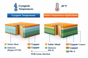
1. Materials Selection for Cryogenic Performance
Traditional FR-4 or standard high-speed substrates are unsuitable. At cryogenic temperatures:
- Material dielectric constants shift.
- Thermal contraction varies between layers.
- Some materials become brittle.
Designers must select and qualify materials (e.g., PTFE composites, Rogers laminates) that maintain stable electrical properties while tolerating extreme thermal cycles.
2. Signal Integrity at the Quantum Scale
Unlike GHz digital signals, quantum control signals may be in the MHz range but are exceptionally sensitive to attenuation and distortion.
PCB design must address:
- Controlled impedance transmission lines
- Ground isolation to prevent cross talk
- Shielded differential pairs
- Microstrip and stripline optimizations
This requires advanced simulation tools and precise manufacturing tolerances.
3. Managing Thermal Gradients and Mechanical Stress
Heat is enemy number one in quantum systems. PCBs are often thermally anchored at multiple temperature stages:
- 300K to 4K transitions
- 4K to millikelvin stages
This introduces mechanical stress due to differential contraction. Thermal modeling and mechanical design rules are essential to prevent delamination or trace cracking.

4. Minimizing Electromagnetic Interference (EMI)
Even slight electromagnetic interference can decohere qubits. PCB designers must:
- Use dedicated ground planes
- Employ careful shielding strategies
- Segregate high-frequency classical signals from quantum control lines
Precision routing and layout reviews are vital to maintain signal purity.
5. Fabrication and Testing Challenges
Producing these PCBs requires:
- Ultra-fine line widths and spacing
- Controlled dielectric thicknesses
- High-reliability vias (e.g., laser drilled, filled)
- Rigorous quality inspection (X-ray, AOI, electrical)
Testing at cryogenic temperatures is also necessary, which introduces specialized test fixtures and protocols.
How Precision4PCB Supports Quantum PCB Development
At Precision4PCB, we leverage:
- Material expertise to guide substrate selection for extreme environments
- Advanced CAM and fabrication for ultra-fine geometry and multilayer designs
- Thermal and signal simulations to validate designs prior to fabrication
- Prototyping services with high-precision tolerances
- Collaborative engineering support to refine designs for manufacturability
Whether you are developing quantum control electronics or cryogenic interposers, our team can p artner with you through every development stage.
Case Study: Quantum Control Board Prototype
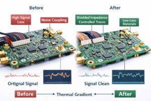
Problem: High signal loss and noise coupling in early prototypes.
Solution: Redesign with optimized ground planes, low-loss materials, and matched impedance lines.
Result: Measurable improvements in signal fidelity at target frequencies and improved cryogenic performance.