The Rise of 3D-Printed PCBs: Are They the Future?
Exploring Advancements in Additive Manufacturing for PCBs
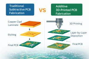
Over the past few years, the printed circuit board (PCB) manufacturing landscape has quietly entered a period of significant evolution. Traditional subtractive manufacturing – etching copper laminates – has been the industry backbone for decades. But now, additive manufacturing techniques, particularly 3D printing for PCBs, are emerging as a credible alternative for prototype production and, potentially, scaled manufacturing.
In this post, we’ll explore what 3D-printed PCBs are, how the technology works, why it’s generating buzz, and what it could mean for the future of electronics manufacturing. We’ll also cover real-world challenges, practical use cases, industry ramifications, and what engineers and buyers should watch for.
1. What Are 3D-Printed PCBs?
At its core, 3D-printed PCBs refer to circuit boards created using additive manufacturing processes – building up conductive and dielectric materials layer by layer using controlled deposition, often guided by digital designs.
Unlike traditional PCBs, which are made through a series of subtractive steps (etching copper from laminate), 3D printing places material only where it’s needed. This brings several potential advantages:
- Faster prototyping turn-arounds
- Potentially less waste
- Complex geometry that may not be possible with traditional fabrication
- Integration of non-planar structures
But what does this mean in practice?
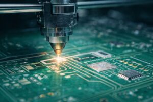
2. How Does 3D PCB Printing Actually Work?
There are multiple additive manufacturing techniques being explored for PCBs, including:
a. Direct Ink Writing (DIW)
Conductive and insulating inks are extruded through a nozzle, depositing one pattern at a time based on digital instructions.
b. Aerosol Jet Printing
Fine droplets of conductive inks are sprayed and directed precisely via a focused aerosol stream – useful for very fine features.
c. Laser-Assisted Additive Manufacturing
Lasers sinter or cure material in targeted zones – ideal for high precision and multi-material printing.
Through these methods, conductive pathways, vias, and insulating layers are built up sequentially, essentially assembling the PCB from the ground up.
3. Why the Interest Now?
Historically, PCB 3D printing was more science-project than viable manufacturing technology. But advances in materials science and additive manufacturing resolution have changed the landscape:
- Conductive inks with better conductivity
- Multi-material print heads
- Integration with CAD/EDA tools for seamless data flow
- Rapid prototype-to-functional board turnaround
- Lower barriers to entry for low-volume runs
Engineers value speed and flexibility. As prototype complexity increases, 3D printing may deliver benefits that traditional techniques struggle to match.
4. Key Advantages of 3D-Printed PCBs
- Speed and Flexibility
Rapid, single-step creation of prototype boards can slash development cycles. - Custom Geometries
3D printing isn’t limited to flat layers: future boards may include vertical interconnects, embedded components, and non-planar circuitry. - Reduced Wastage
Only the materials needed are deposited, reducing material waste compared to copper etching processes. - On-Demand Production Potential
For low-volume or custom boards, on-demand 3D printing could reduce inventory and accelerate delivery.
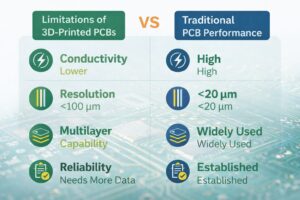
5. Challenges and Limitations That Still Remain
Despite its promise, 3D-printed PCBs face real barriers before they can replace conventional methods:
- Conductivity and Performance
3D-printed conductive inks often do not yet match the copper conductivity achieved in traditional boards, which can impact high-frequency and high-current performance. - Resolution & Precision
Fine features (e.g., tight trace spacing, microvias below 50 μm) remain difficult for many 3D printing systems. - Material Compatibility
Integrating high-performance dielectrics, multilayer stackups, and embedded passive components is still more practical with traditional processes. - Testing & Reliability
Industry-standard reliability testing (thermal cycling, mechanical shock, high-frequency testing) needs broader data on 3D printed boards.
6. Use Cases Where 3D-Printed PCBs Are Already Valuable
Even if they’re not replacing conventional PCBs yet, 3D-printed PCBs are already finding traction in:
- Rapid Prototyping
Near-instant boards for proof of concept and early prototype testing. - Educational and Research Settings
Fast board creation for labs, universities, and development teams. - Low-Volume Custom Electronics
Where turnaround time matters more than peak electrical performance. - Sensor Integration & IoT
Custom shapes and embedded features via additive techniques.
7. Future Directions: What’s on the Horizon?
Experts believe the future of PCB printing could include:
- Embedded Passive Components
Resistors and capacitors printed directly into the board substrate. - 3D Interconnects
Multi-planar circuits that don’t rely on drilled vias. - Smart Boards
Integration of sensors, antennas, and thermal management structures during fabrication. - Hybrid Manufacturing
Traditional boards enhanced with printed features that improve performance, without full 3D print replacement.
8. What This Means for Precision4PCB and PCB Buyers
At Precision4PCB, we believe innovation should complement reliability. 3D-printed PCBs represent a fascinating avenue for rapid prototyping and custom electronics – but traditional high-performance PCB fabrication remains essential for most commercial and industrial applications.
This technology may mature to augment existing services, especially for early prototyping and low-volume custom runs.