- October 23, 2025
- PCB Design, PCB Manufacturing
AI and Machine Learning in PCB Design and Manufacturing
How Artificial Intelligence is Transforming Layout Optimization and Defect Detection in Modern Electronics.
In the fast-evolving electronics industry, the demand for smaller, faster, and more efficient PCBs is growing rapidly. Traditional design and manufacturing methods are reaching their limits – and that’s where Artificial Intelligence (AI) and Machine Learning (ML) are reshaping the game.
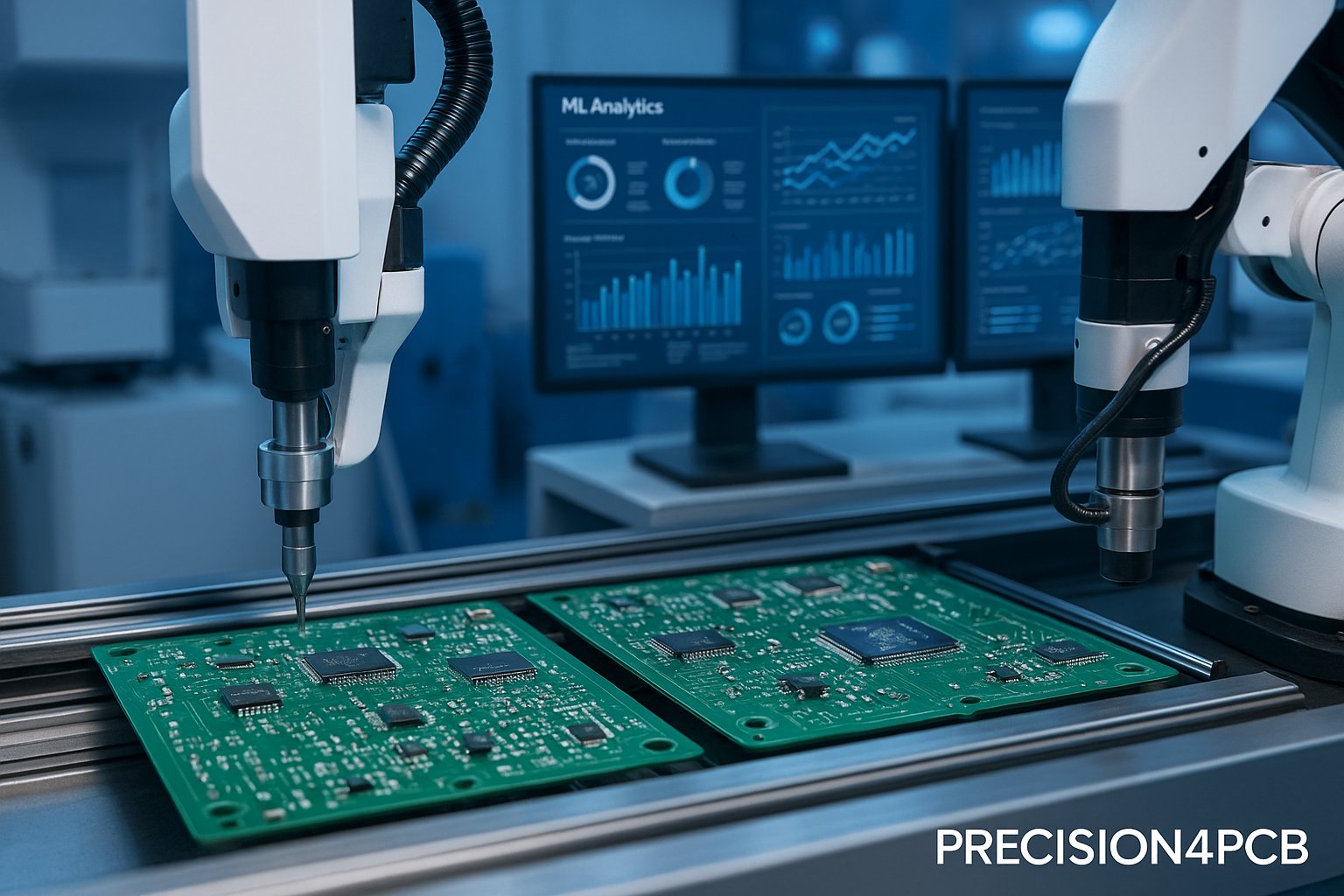
At Precision4PCB, we’re leveraging AI-driven tools and data intelligence to push the boundaries of PCB design accuracy, manufacturing efficiency, and defect detection, ensuring unmatched quality and reliability in every board we deliver.
Table of Contents
- Introduction: The New Era of PCB Design
- How AI Is Revolutionizing PCB Design
- Layout Optimization
- Component Placement and Routing
- Signal Integrity and Thermal Analysis
- Machine Learning in PCB Manufacturing
- Predictive Quality Control
- Automated Optical Inspection (AOI)
- Real-Time Process Optimization
- Benefits of AI Integration in PCB Processes
- Challenges in Adopting AI and ML
- Precision4PCB’s AI-Enhanced Manufacturing Approach
- Conclusion
- FAQs
Introduction: The New Era of PCB Design
Printed Circuit Boards (PCBs) are the heart of every electronic product. However, as devices become more complex, manual design and inspection methods struggle to keep up with tight tolerances and high-density layouts.
This is where AI and Machine Learning are transforming PCB engineering. These technologies bring data-driven intelligence to every stage – from schematic design and layout optimization to manufacturing quality control.
How AI Is Revolutionizing PCB Design
AI doesn’t replace human designers – it augments them. By processing vast datasets and analyzing design rules, AI can optimize board layouts, enhance routing, and even predict performance issues before manufacturing begins.
1. Layout Optimization
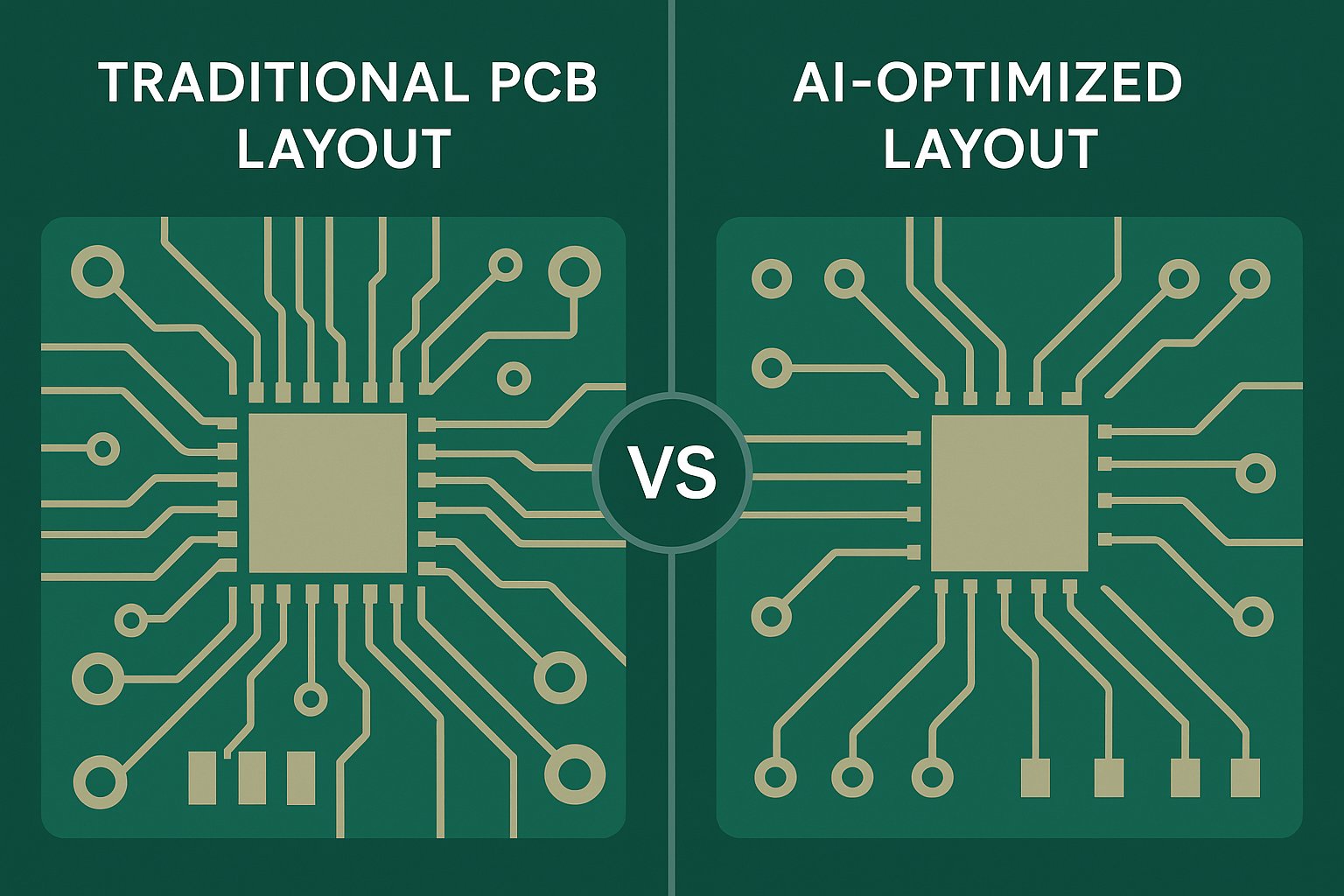
AI-powered design tools use algorithms to evaluate thousands of possible layout configurations in seconds. These tools identify optimal component placement, routing paths, and trace widths to minimize crosstalk, EMI, and power loss.
Key Advantages:
- Reduces manual trial and error
- Improves signal and power integrity
- Minimizes board area without compromising performance
2. Component Placement and Routing
Machine learning models learn from historical designs and successful routing patterns to automate placement and routing decisions. This results in faster design cycles and fewer human errors.
Example:
AI can automatically place high-frequency components near ground planes or suggest optimal via placements to reduce impedance mismatches.
3. Signal Integrity and Thermal Analysis
AI-driven simulations predict signal distortions, hotspots, and thermal issues early in the design phase.
By integrating AI thermal models, engineers can detect heat accumulation areas and modify designs before prototyping, saving time and costs.
Machine Learning in PCB Manufacturing
Beyond design, machine learning plays a critical role in PCB fabrication, assembly, and inspection.
ML algorithms continuously learn from production data to detect defects, predict failures, and optimize manufacturing parameters in real time.
1. Predictive Quality Control
Machine learning models analyze historical defect data, solder profiles, and machine behavior to predict potential issues before they occur.
Benefits:
- Prevents costly rework
- Improves yield rates
- Ensures consistent quality control
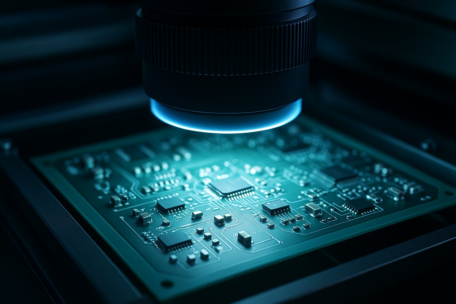
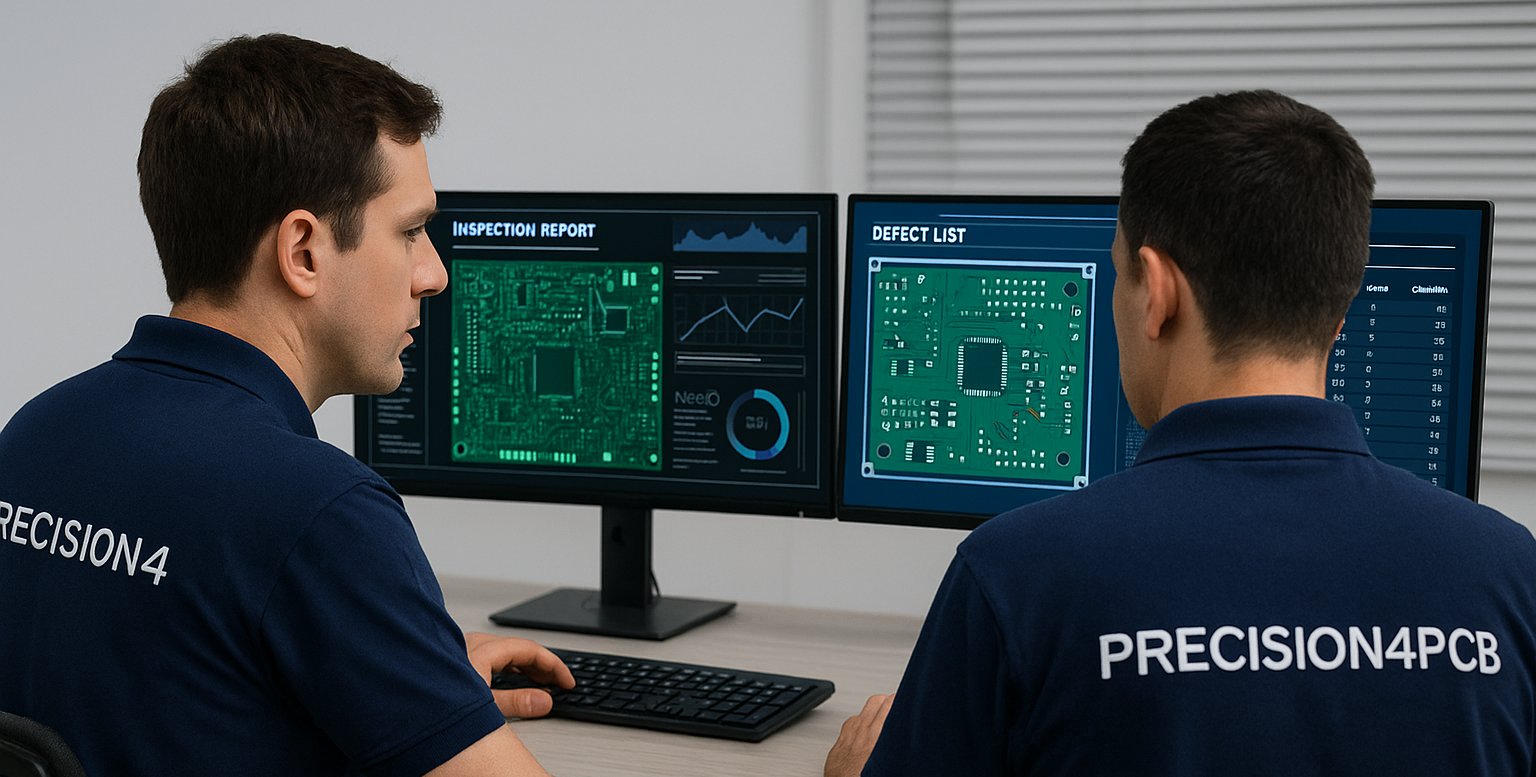
2. Automated Optical Inspection (AOI)
AI-enhanced AOI systems use computer vision to identify micro-defects that are nearly impossible to detect manually.
These include:
- Hairline solder cracks
- Misaligned components
- Insufficient solder joints
- Microvia irregularities
Modern AOI systems at Precision4PCB achieve over 99% defect detection accuracy using ML-driven pattern recognition.
3. Real-Time Process Optimization
ML algorithms monitor real-time production metrics (temperature, humidity, soldering profiles, etc.) and automatically adjust parameters to maintain process stability.
This ensures precision assembly even in complex multilayer boards.
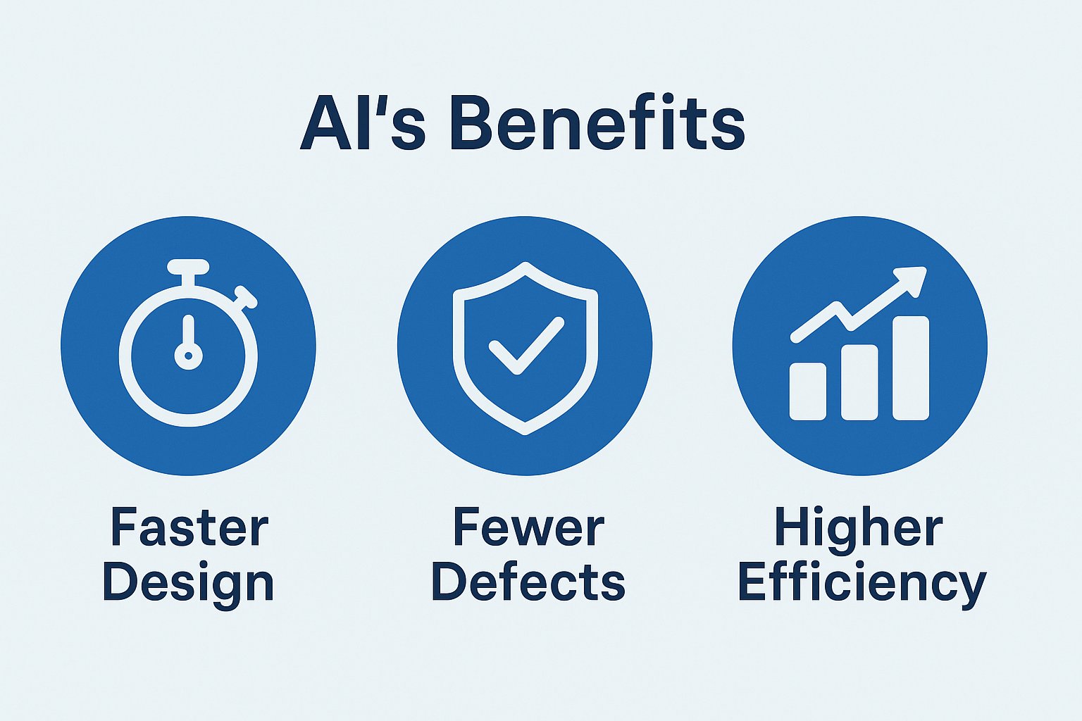
Benefits of AI Integration in PCB Processes
AI and ML offer tangible improvements across the design-to-production pipeline:
| Area | Traditional Process | AI-Driven Process |
|---|---|---|
| Design Time | Manual routing, time-intensive | Automated, adaptive optimization |
| Quality Control | Human inspection | AI-based defect recognition |
| Yield Rate | Reactive problem-solving | Predictive maintenance |
| Cost Efficiency | High rework cost | Reduced waste and downtime |
Challenges in Adopting AI and ML
While the advantages are immense, implementing AI and ML in PCB manufacturing comes with challenges:
- Data Quality: AI depends on accurate and clean production data.
- Integration Complexity: Requires aligning AI tools with existing EDA (Electronic Design Automation) software.
- Expertise Gap: Engineers must adapt to data-driven design workflows.
Precision4PCB addresses these through training, process standardization, and advanced tool integration.
Precision4PCB’s AI-Enhanced Manufacturing Approach
At Precision4PCB, innovation drives everything we do.
Our AI-powered design and inspection systems allow us to deliver higher-quality PCBs, faster and more cost-effectively.
Our AI initiatives include:
- AI-assisted layout design for dense, multilayer boards
- Machine-learning-driven AOI and X-ray inspection for micro-defect detection
- Data analytics integration for real-time process control
- Predictive maintenance to reduce production downtime
Conclusion
The integration of AI and Machine Learning in PCB design and manufacturing isn’t just a future trend – it’s the present reality.
By automating complex processes, predicting potential failures, and optimizing layouts, AI empowers manufacturers to achieve precision, speed, and cost efficiency like never before.
At Precision4PCB, we are at the forefront of this technological revolution, using AI-powered intelligence to build the next generation of high-performance PCBs.
Ready to experience AI-powered precision in PCB manufacturing?
Let our engineering experts help you design smarter, build faster, and deliver better.
Contact Precision4PCB today to get a free project consultation or AI-based design review.
Frequently Asked Questions (FAQs)
AI analyzes complex electrical and mechanical constraints to automatically suggest optimal routing paths, component placement, and thermal balancing – significantly reducing manual design time.
Machine learning models identify patterns in defects, allowing early detection and correction of potential issues in soldering, vias, or alignment before boards reach final assembly.
Yes. AI minimizes rework, improves process accuracy, and optimizes resource usage — resulting in lower production costs and higher yields.
Precision4PCB integrates AI across layout optimization, inspection, and predictive analytics to deliver consistent, high-quality PCBs efficiently and reliably.
AI will play a bigger role in autonomous design, adaptive testing, and fully self-optimizing production lines, creating a new era of smart, data-driven electronics manufacturing.

