- October 20, 2025
- PCB Blog
How to Optimize PCB Panelization for Cost and Efficiency
In PCB manufacturing, panelization is one of the most overlooked – yet most impactful – steps in optimizing production cost, speed, and material efficiency. By smartly arranging multiple PCBs onto a single manufacturing panel, manufacturers can minimize waste, reduce assembly time, and enhance yield consistency.
At Precision4PCB, we emphasize design strategies that ensure every square inch of your PCB panel delivers maximum efficiency – without compromising quality.
Let’s explore what PCB panelization is, why it’s important, and the best practices to make it both cost-effective and production-friendly.
Table of Contents
- What Is PCB Panelization?
- Why PCB Panelization Matters
- Common Panelization Methods
- Best Practices for Optimizing PCB Panelization
- Design Guidelines for Cost and Efficiency
- Precision4PCB’s Approach to Smart Panelization
- Conclusion
- FAQs
What Is PCB Panelization?
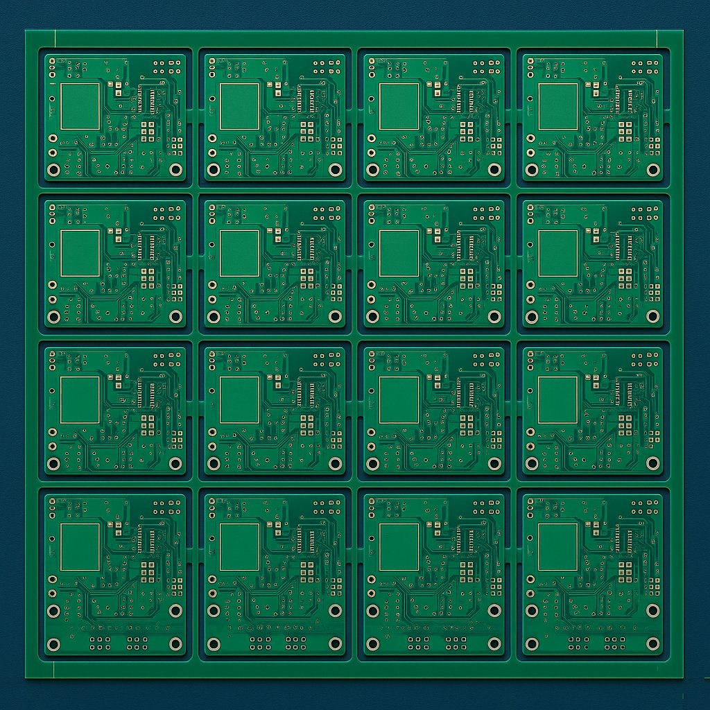
PCB panelization is the process of grouping multiple smaller circuit boards together into a larger panel, allowing them to be fabricated and assembled simultaneously. Once assembly and testing are complete, individual boards are separated – or de-panelized – for use.
Why It’s Done
- To streamline assembly on pick-and-place machines
- To reduce handling and production time
- To minimize material waste during fabrication
- To protect smaller PCBs during processing
Why PCB Panelization Matters
Effective panelization can make the difference between a profitable project and a costly one. Optimized panels:
- Increase fabrication yield
- Improve machine utilization
- Reduce assembly and setup time
- Prevent mechanical stress or warping during manufacturing
- Lower material and operational costs
Common Panelization Methods
There are several ways to design PCB panels, each suited to different board types, shapes, and manufacturing needs.
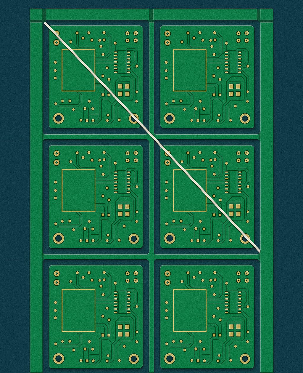
1. V-Scoring
- PCBs are separated using V-shaped grooves scored on both sides of the board.
- Ideal for straight-edged boards.
- Pros: Simple, cost-effective, easy for automated depaneling.
- Cons: Not suitable for irregular board shapes.
2. Tab-Route Panelization
- PCBs are joined with small tabs (breakaway points) along their edges.
- Tabs may include mouse bites (small perforations) for easier snapping.
- Pros: Great for irregular or round PCBs.
- Cons: May leave rough edges or require sanding.
3. Combination Method
- Mixes V-scoring and tab-routing for complex boards that need additional support during manufacturing.
- Common in multilayer, flexible, or odd-shaped designs.
Best Practices for Optimizing PCB Panelization
1. Match Panel Size to Fabricator’s Standard
Fabricators often have standard panel sizes (e.g., 18″ x 24″, 19″ x 31″) to fit their machinery.
Using these sizes efficiently minimizes material waste and tooling costs.
Tip: Consult your manufacturer early – like Precision4PCB – to design around optimal panel dimensions.
2. Align Components with Assembly Process
Keep all PCBs in the panel oriented the same way. This ensures:
- Consistent pick-and-place programming
- Fewer rotation adjustments
- Faster assembly cycles
3. Maintain Uniform Spacing
Allow proper clearance (typically 2-3 mm) between individual boards.
This spacing supports clean routing, avoids copper exposure, and allows smooth depaneling.
4. Use Fiducials and Tooling Holes
Add global and local fiducials for alignment and optical recognition during assembly.
Also, tooling holes help accurately position panels on conveyor belts.
5. Optimize Tab Placement
Strategically place tabs away from:
- Connectors
- SMD pads
- Mounting holes
This prevents stress fractures or pad lifting during depaneling.
6. Ensure Panel Stability
Add support rails or frames for small or thin boards to prevent bending during reflow soldering or transport.
7. Account for Depaneling Stress
Choose the right depaneling technique – mechanical, laser, or router – based on board fragility.
Improper depaneling can cause cracks or solder joint damage.
Design Guidelines for Cost and Efficiency
| Design Factor | Recommendation | Benefit |
|---|---|---|
| Panel Size | Match with manufacturer’s standard | Reduces material waste |
| Board Spacing | 2–3 mm gap | Safe routing and cutting |
| Fiducials | 3 global + 2 local per board | Accurate placement |
| Rail Width | 5–10 mm | Panel strength during reflow |
| Tab Count | Minimum for strength | Easier depaneling |
| Component Orientation | Consistent | Faster assembly setup |
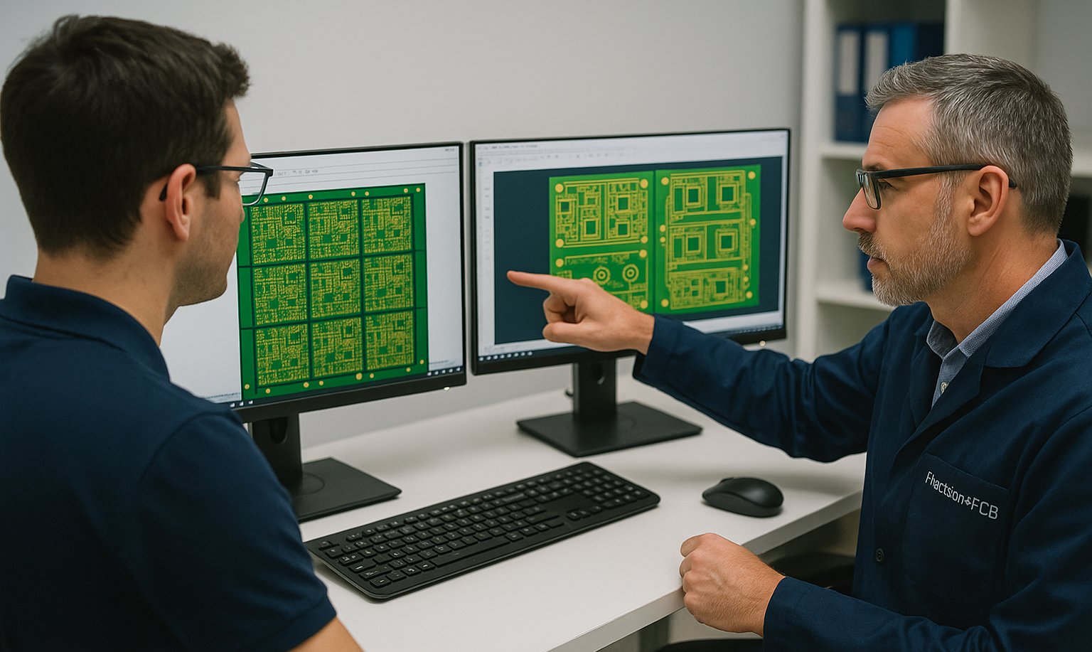
Precision4PCB’s Approach to Smart Panelization
At Precision4PCB, we use engineering-driven design optimization to ensure your PCB panels deliver the highest yield at the lowest cost.
Our design team evaluates:
- Panel layout efficiency and yield rate
- Depaneling strategy and mechanical stress
- Thermal behavior during reflow
- Routing paths for minimal waste
With advanced CAM software and DFM analysis, we help customers achieve faster turnarounds, consistent quality, and lower production costs – from prototype to full-scale manufacturing.
Conclusion
Optimizing PCB panelization isn’t just a design exercise – it’s a strategic decision that influences your cost, yield, and efficiency throughout the entire production cycle.
By applying the right panelization methods and following best practices, manufacturers can save material, speed up assembly, and ensure top-tier reliability.
Partner with Precision4PCB, where we bring engineering expertise and cutting-edge automation to every project – making your PCB production both precise and cost-efficient.
Ready to make your PCB manufacturing more efficient and cost-effective?
Our experts at Precision4PCB can help you optimize your design for maximum yield and minimal waste.
Contact us today for a free panelization design review or to discuss your next project.

Frequently Asked Questions (FAQs)
It depends on your manufacturer’s equipment. At Precision4PCB, common panel sizes are 18” x 24” and 19” x 31”, though we adjust based on the project and efficiency goals.
By combining multiple PCBs into one panel, you save on setup, handling, and material costs while increasing throughput on automated machines.
V-scoring: Best for rectangular boards.
Tab-routing: Ideal for irregular shapes or when smoother edges are required.
Precision4PCB often uses a hybrid approach for optimal results.
Use proper tab placement, maintain clearance from components, and choose laser or router depaneling for delicate multilayer designs.
Absolutely. Our engineering team can analyze your current panel design and recommend layout or spacing improvements that reduce cost, increase yield, and enhance production speed.