- June 3, 2026
- PCB Blog, PCB Design, PCB Manufacturing
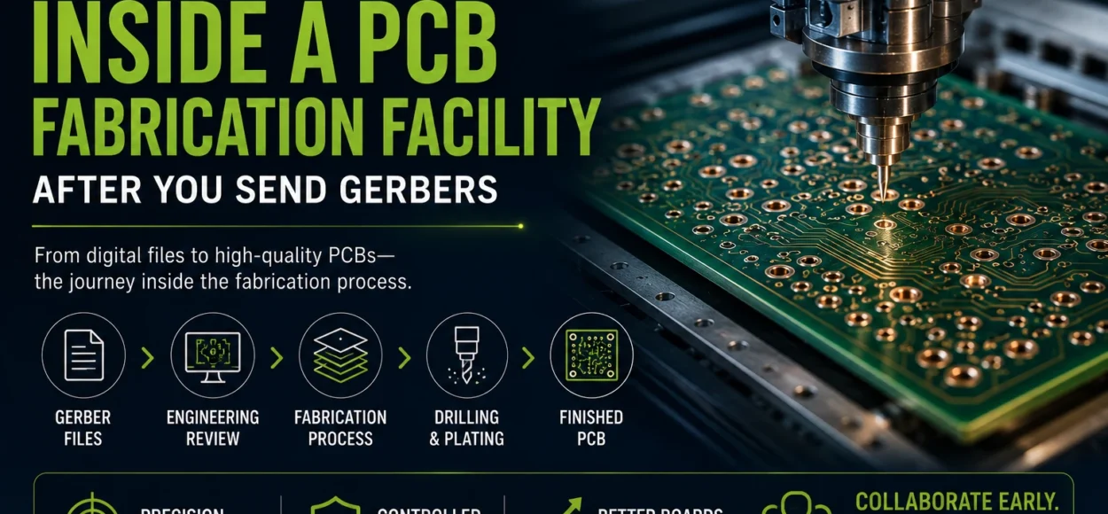
What Happens Inside a PCB Fabrication Facility After You Send Gerbers
When engineers release Gerber files for a printed circuit board, the design often feels complete. In reality, that is when the manufacturing journey begins. Inside a PCB fabrication facility, a series of precise and tightly controlled processes transform those digital files into a physical circuit board. Understanding what happens during this process helps engineers design boards that build correctly the first time.
The first step after receiving Gerbers is engineering review and data preparation. Fabrication engineers analyze the design to verify manufacturability. They check trace widths, spacing, annular rings, drill sizes, and layer alignment against the capabilities of the manufacturing process. At this stage, potential issues such as overly fine features, tight spacing, or challenging stackups may be flagged.
Once the design passes review, the manufacturing process begins with material preparation. Copper-clad laminate panels are selected according to the stackup defined in the design. These panels form the base material on which the circuits will be created.
The next step is imaging. Using photoresist and laser or UV imaging systems, the copper pattern from the Gerber data is transferred onto the panel. This step defines the exact trace geometry that will form the electrical pathways. Imaging precision is critical because even small deviations can affect impedance control, signal integrity, and overall electrical performance.
After imaging comes etching. Chemical processes remove the unwanted copper, leaving only the designed traces and pads. However, etching is not perfectly vertical. Slight sidewall erosion can occur, which means the final trace width may differ slightly from the design. These fabrication tolerances are one of the reasons controlled impedance calculations must account for real manufacturing conditions.
Drilling follows, creating holes for vias and component leads. Modern PCB facilities use high-speed CNC drilling machines capable of extremely tight positional accuracy. After drilling, the holes are plated with copper to create electrical connections between layers.
Plating is another critical stage. Copper electroplating thickens traces and builds conductive material inside drilled holes. The thickness of this plating influences electrical resistance and reliability, particularly in high-current or high-reliability applications.
Some layouts are inherently more difficult to manufacture than others. Extremely fine lines, dense via fields, uneven copper distribution, and complex stackups all increase process complexity and risk.
The best way engineers can ensure success is by designing with fabrication realities in mind. Collaborating with the PCB fabricator early in the design process helps align stackups, tolerances, and materials with real manufacturing capabilities.
When engineers understand what happens inside the fabrication facility, they design smarter boards—and prototypes succeed the first time.
For more information go to www.precision4pcb.com or call the president Jay Rupani at 847-439-5447 and he’ll be happy to help you out.